SLASF99 December   2023 TAS5827

PRODUCTION DATA  

  1.   1
  2. Features
  3. Applications
  4. Description
  5. Pin Configuration and Functions
  6. Specifications
    1. 5.1 Absolute Maximum Ratings
    2. 5.2 ESD Ratings
    3. 5.3 Recommended Operating Conditions
    4. 5.4 Thermal Information
    5. 5.5 Electrical Characteristics
    6. 5.6 Timing Requirements
    7. 5.7 Typical Characteristics
      1. 5.7.1 Bridge Tied Load (BTL) Configuration Curves with BD Modulation
      2. 5.7.2 Bridge Tied Load (BTL) Configuration Curves with 1SPW Modulation
      3. 5.7.3 Parallel Bridge Tied Load (PBTL) Configuration With BD Modulation
      4. 5.7.4 Parallel Bridge Tied Load (PBTL) Configuration With 1SPW Modulation
  7. Detailed Description
    1. 6.1 Overview
    2. 6.2 Functional Block Diagram
    3. 6.3 Feature Description
      1. 6.3.1 Power Supplies
      2. 6.3.2 Device Clocking
      3. 6.3.3 Serial Audio Port – Clock Rates
      4. 6.3.4 Clock Halt Auto-recovery
      5. 6.3.5 Sample Rate on the Fly Change
      6. 6.3.6 Serial Audio Port - Data Formats and Bit Depths
    4. 6.4 Device Functional Modes
      1. 6.4.1 Software Control
      2. 6.4.2 Speaker Amplifier Operating Modes
        1. 6.4.2.1 BTL Mode
        2. 6.4.2.2 PBTL Mode
      3. 6.4.3 Low EMI Modes
        1. 6.4.3.1 Spread Spectrum
        2. 6.4.3.2 Channel to Channel Phase Shift
        3. 6.4.3.3 Multi-Devices PWM Phase Synchronization
          1. 6.4.3.3.1 Phase Synchronization With I2S Clock In Startup Phase
          2. 6.4.3.3.2 Phase Synchronization With GPIO
      4. 6.4.4 Thermal Foldback
      5. 6.4.5 Device State Control
      6. 6.4.6 Device Modulation
        1. 6.4.6.1 BD Modulation
        2. 6.4.6.2 1SPW Modulation
        3. 6.4.6.3 Hybrid Modulation
      7. 6.4.7 Programming and Control
        1. 6.4.7.1 I2C Serial Communication Bus
        2. 6.4.7.2 Hardware Control Mode
        3. 6.4.7.3 I2C Target Address
          1. 6.4.7.3.1 Random Write
          2. 6.4.7.3.2 Sequential Write
          3. 6.4.7.3.3 Random Read
          4. 6.4.7.3.4 Sequential Read
          5. 6.4.7.3.5 DSP Memory Book, Page and BQ update
          6. 6.4.7.3.6 Checksum
            1. 6.4.7.3.6.1 Cyclic Redundancy Check (CRC) Checksum
            2. 6.4.7.3.6.2 Exclusive or (XOR) Checksum
        4. 6.4.7.4 Control via Software
          1. 6.4.7.4.1 Startup Procedures
          2. 6.4.7.4.2 Shutdown Procedures
        5. 6.4.7.5 Protection and Monitoring
          1. 6.4.7.5.1 Overcurrent Limit (Cycle-By-Cycle)
          2. 6.4.7.5.2 Overcurrent Shutdown (OCSD)
          3. 6.4.7.5.3 DC Detect Error
          4. 6.4.7.5.4 Overtemperature Shutdown (OTSD)
          5. 6.4.7.5.5 PVDD Overvoltage and Undervoltage Error
          6. 6.4.7.5.6 PVDD Drop Detection
          7. 6.4.7.5.7 Clock Fault
    5. 6.5 Register Maps
      1. 6.5.1 reg_map Registers
  8. Application and Implementation
    1. 7.1 Typical Applications
      1. 7.1.1 2.0 (Stereo BTL) System
      2. 7.1.2 Mono (PBTL) Systems
      3. 7.1.3 Layout Guidelines
        1. 7.1.3.1 General Guidelines for Audio Amplifiers
        2. 7.1.3.2 Importance of PVDD Bypass Capacitor Placement on PVDD Network
        3. 7.1.3.3 Optimizing Thermal Performance
          1. 7.1.3.3.1 Device, Copper, and Component Layout
          2. 7.1.3.3.2 Stencil Pattern
          3. 7.1.3.3.3 PCB footprint and Via Arrangement
          4. 7.1.3.3.4 Solder Stencil
        4. 7.1.3.4 Layout Example
  9. Power Supply Recommendations
    1. 8.1 DVDD Supply
    2. 8.2 PVDD Supply
  10. Device and Documentation Support
    1. 9.1 Device Support
      1. 9.1.1 Device Nomenclature
      2. 9.1.2 Development Support
    2. 9.2 Receiving Notification of Documentation Updates
    3. 9.3 Support Resources
    4. 9.4 Trademarks
    5. 9.5 Electrostatic Discharge Caution
    6. 9.6 Glossary
  11. 10Revision History
  12. 11Mechanical, Packaging, and Orderable Information

Package Options

Mechanical Data (Package|Pins)
Thermal pad, mechanical data (Package|Pins)
Orderable Information

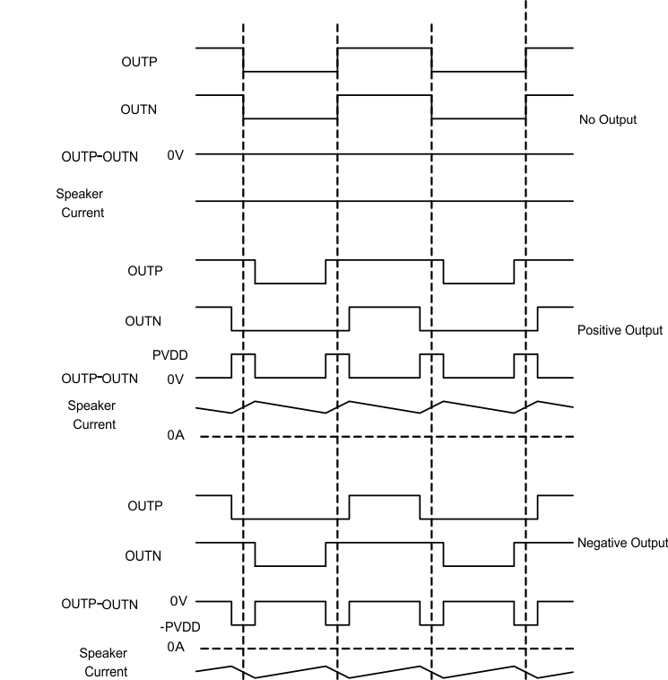
BD Modulation

This is a modulation scheme that allows operation without the classic LC reconstruction filter when the amp is driving an inductive load with short speaker wires. Each output is switching from 0 volts to the supply voltage. The OUTPx and OUTNx are in phase with each other with no input so there is little or no current in the speaker. The duty cycle of OUTPx is greater than 50% and OUTNx is less than 50% for positive output voltages. The duty cycle of OUTPx is less than 50% and OUTNx is greater than 50% for negative output voltages. The voltage across the load sits at 0 V throughout most of the switching period, reducing the switching current, which reduces any I2R losses in the load.
GUID-EEC24F74-50B8-4C28-BB3D-D6B05B3720B9-low.gifFigure 6-8 BD Mode Modulation