SLLSFL9A July   2021  – December 2021 TCAN1046A-Q1

PRODUCTION DATA  

  1. Features
  2. Applications
  3. Description
  4. Revision History
  5. Pin Configuration and Functions
  6. Specifications
    1. 6.1  Absolute Maximum Ratings
    2. 6.2  ESD Ratings
    3. 6.3  ESD Ratings — IEC Specifications
    4. 6.4  Recommended Operating Conditions
    5. 6.5  Thermal Characteristics
    6. 6.6  Supply Characteristics
    7. 6.7  Dissipation Ratings
    8. 6.8  Electrical Characteristics
    9. 6.9  Switching Characteristics
    10. 6.10 Typical Characteristics
  7. Parameter Measurement Information
  8. Detailed Description
    1. 8.1 Overview
    2. 8.2 Functional Block Diagram
    3. 8.3 Feature Description
      1. 8.3.1 Pin Description
        1. 8.3.1.1 TXD1 and TXD2
        2. 8.3.1.2 GND1 and GND2
        3. 8.3.1.3 VCC1 and VCC2
        4. 8.3.1.4 RXD1 and RXD2
        5. 8.3.1.5 CANH1, CANL1, CANH2, and CANL1
        6. 8.3.1.6 STB1 and STB2 (Standby)
      2. 8.3.2 CAN Bus States
      3. 8.3.3 TXD Dominant Timeout (DTO)
      4. 8.3.4 CAN Bus Short-Circuit Current Limiting
      5. 8.3.5 Thermal Shutdown (TSD)
      6. 8.3.6 Undervoltage Lockout
      7. 8.3.7 Unpowered Device
      8. 8.3.8 Floating pins
    4. 8.4 Device Functional Modes
      1. 8.4.1 Operating Modes
      2. 8.4.2 Normal Mode
      3. 8.4.3 Standby Mode
        1. 8.4.3.1 Remote Wake Request via Wake-Up Pattern (WUP) in Standby Mode
      4. 8.4.4 Driver and Receiver Function
  9. Application and Implementation
    1. 9.1 Application Information
    2. 9.2 Typical Application
      1. 9.2.1 Design Requirements
        1. 9.2.1.1 CAN Termination
      2. 9.2.2 Detailed Design Procedures
        1. 9.2.2.1 Bus Loading, Length and Number of Nodes
      3. 9.2.3 Application Curves
  10. 10Power Supply Recommendations
  11. 11Layout
    1. 11.1 Layout Guidelines
    2. 11.2 Layout Example
  12. 12Device and Documentation Support
    1. 12.1 Receiving Notification of Documentation Updates
    2. 12.2 Support Resources
    3. 12.3 Trademarks
    4. 12.4 Electrostatic Discharge Caution
    5. 12.5 Glossary

Package Options

Mechanical Data (Package|Pins)
Thermal pad, mechanical data (Package|Pins)
Orderable Information

CAN Bus States

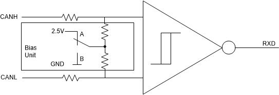
The CAN bus has two logical states during operation: recessive and dominant. See Figure 8-2 and Figure 8-3.

A dominant bus state occurs when the bus is driven differentially and corresponds to a logic low on the TXD1, TXD2, RXD1 and RXD2 pins. A recessive bus state occurs when the bus is biased to VCC/2 via the high-resistance internal input resistors (RIN) of the receiver and corresponds to a logic high on the TXD1, TXD2, RXD1 and RXD2 pins.

A dominant state overwrites the recessive state during arbitration. Multiple CAN nodes may be transmitting a dominant bit at the same time during arbitration, and in this case the differential voltage of the bus is greater than the differential voltage of a single driver.

The TCAN1046A-Q1 transceiver implements a low-power standby (STB) mode which enables a third bus state where the bus pins are weakly biased to ground via the high resistance internal resistors of the receiver. See Figure 8-2 and Figure 8-3.
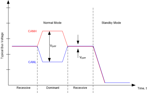
GUID-C66E5CA0-7273-44CF-95C7-F7F9F462A7E6-low.gif Figure 8-2 Bus States
GUID-07D29E54-C27C-403C-960B-C8A606FC4E42-low.gif
Normal Mode
Standby Mode
Figure 8-3 Simplified Recessive Common Mode Bias Unit and Receiver