SLLSFV9 July   2024 TCAN1473-Q1

ADVANCE INFORMATION  

  1.   1
  2. Features
  3. Applications
  4. Description
  5. Pin Configuration and Functions
  6. Specifications
    1. 5.1  Absolute Maximum Ratings
    2. 5.2  ESD Ratings
    3. 5.3  ESD Ratings - IEC Specifications
    4. 5.4  Recommended Operating Conditions
    5. 5.5  Thermal Information
    6. 5.6  Power Dissipation Ratings
    7. 5.7  Power Supply Characteristics
    8. 5.8  Electrical Characteristics
    9. 5.9  Timing Requirements
    10. 5.10 Switching Characteristics
  7. Parameter Measurement Information
  8. Detailed Description
    1. 7.1 Overview
      1. 7.1.1 Signal Improvement
    2. 7.2 Functional Block Diagram
    3. 7.3 Feature Description
      1. 7.3.1 Supply Pins
        1. 7.3.1.1 VSUP Pin
        2. 7.3.1.2 VCC Pin
        3. 7.3.1.3 VIO Pin
      2. 7.3.2 Digital Inputs and Outputs
        1. 7.3.2.1 TXD Pin
        2. 7.3.2.2 RXD Pin
        3. 7.3.2.3 nFAULT Pin
        4. 7.3.2.4 EN Pin
        5. 7.3.2.5 nSTB Pin
      3. 7.3.3 GND
      4. 7.3.4 INH Pin
      5. 7.3.5 WAKE Pin
      6. 7.3.6 CAN Bus Pins
      7. 7.3.7 Faults
        1. 7.3.7.1 Internal and External Fault Indicators
          1. 7.3.7.1.1 Power-Up (PWRON Flag)
          2. 7.3.7.1.2 Wake-Up Request (WAKERQ Flag)
          3. 7.3.7.1.3 Undervoltage Faults
            1. 7.3.7.1.3.1 Undervoltage on VSUP
            2. 7.3.7.1.3.2 Undervoltage on VCC
            3. 7.3.7.1.3.3 Undervoltage on VIO
          4. 7.3.7.1.4 CAN Bus Fault (CBF Flag)
          5. 7.3.7.1.5 TXD Dominant State Timeout (TXDDTO Flag)
          6. 7.3.7.1.6 TXD Shorted to RXD Fault (TXDRXD Flag)
          7. 7.3.7.1.7 CAN Bus Dominant Fault (CANDOM Flag)
      8. 7.3.8 Local Faults
        1. 7.3.8.1 TXD Dominant Timeout (TXD DTO)
        2. 7.3.8.2 Thermal Shutdown (TSD)
        3. 7.3.8.3 Undervoltage Lockout (UVLO)
        4. 7.3.8.4 Unpowered Devices
        5. 7.3.8.5 Floating Terminals
        6. 7.3.8.6 CAN Bus Short-Circuit Current Limiting
    4. 7.4 Device Functional Modes
      1. 7.4.1 Operating Mode Description
        1. 7.4.1.1 Normal Mode
        2. 7.4.1.2 Silent Mode
        3. 7.4.1.3 Standby Mode
        4. 7.4.1.4 Go-To-Sleep Mode
        5. 7.4.1.5 Sleep Mode
          1. 7.4.1.5.1 Remote Wake Request via Wake-Up Pattern (WUP)
          2. 7.4.1.5.2 Local Wake-Up (LWU) via WAKE Input Terminal
      2. 7.4.2 CAN Transceiver
        1. 7.4.2.1 CAN Transceiver Operation
          1. 7.4.2.1.1 CAN Transceiver Modes
            1. 7.4.2.1.1.1 CAN Off Mode
            2. 7.4.2.1.1.2 CAN Autonomous: Inactive and Active
            3. 7.4.2.1.1.3 CAN Active
          2. 7.4.2.1.2 Driver and Receiver Function Tables
          3. 7.4.2.1.3 CAN Bus States
  9. Application Information Disclaimer
    1. 8.1 Application Information
      1. 8.1.1 Typical Application
      2. 8.1.2 Design Requirements
        1. 8.1.2.1 Bus Loading, Length and Number of Nodes
      3. 8.1.3 Detailed Design Procedure
        1. 8.1.3.1 CAN Termination
      4. 8.1.4 Application Curves
    2. 8.2 Power Supply Recommendations
    3. 8.3 Layout
      1. 8.3.1 Layout Guidelines
      2. 8.3.2 Layout Example
  10. Device and Documentation Support
    1. 9.1 Documentation Support
    2. 9.2 Receiving Notification of Documentation Updates
    3. 9.3 Support Resources
    4. 9.4 Trademarks
    5. 9.5 Electrostatic Discharge Caution
    6. 9.6 Glossary
  11. 10Revision History
  12. 11Mechanical, Packaging, and Orderable Information
    1. 11.1 Package Option Addendum
      1. 11.1.1 Packaging Information
      2. 11.1.2 Tape and Reel Information

Package Options

Mechanical Data (Package|Pins)
Thermal pad, mechanical data (Package|Pins)
Orderable Information

Signal Improvement

The TCAN1473-Q1 includes the Signal Improvement Capability (SIC) that enhances the maximum data rate achievable in complex star topologies by minimizing signal ringing. Signal ringing is the result of reflections caused by impedance mismatch at various points in a complex CAN network.

An example of a star network is shown Figure 7-1.
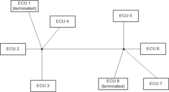
TCAN1473-Q1 CAN network: Star TopologyFigure 7-1 CAN network: Star Topology

Recessive-to-dominant signal edge is usually clean as it’s strongly driven by the transmitter. Transmitter output impedance of CAN transceiver is RID(dom) and matches to the network characteristic impedance. For a regular CAN FD transceiver, dominant-to-recessive edge is when the driver output impedance goes to approximately 60kΩ and signal reflected back experiences impedance mismatch which causes ringing. The TCAN1473-Q1 resolves this issue by TX-based Signal improvement capability (SIC). The TCAN1473-Q1 continues to drive the bus recessive strongly for tSIC_TX_base to minimize the reflections, and the recessive bit is clean at the sampling point. In the active recessive phase, transmitter output impedance is low (RID(active_rec)). After this phase, the device enters into a passive recessive phase where the driver goes into high impedance state. This phenomenon is explained using Figure 7-2. For further information, please refer to the white paper on how SIC unlocks the real potential of CAN-FD transceivers.

TCAN1473-Q1 TX based Signal Improvement CapabilityFigure 7-2 TX based Signal Improvement Capability