SLOS217I July 1998 – December 2024 THS3001
PRODUCTION DATA
- 1
- 1 Features
- 2 Applications
- 3 Description
- 4 Pin Configuration and Functions
- 5 Specifications
- 6 Detailed Description
- 7 Application and Implementation
- 8 Device and Documentation Support
- 9 Revision History
- 10Mechanical, Packaging, and Orderable Information
Package Options
Refer to the PDF data sheet for device specific package drawings
Mechanical Data (Package|Pins)
- D|8
- DGN|8
Thermal pad, mechanical data (Package|Pins)
- DGN|8
Orderable Information
7.2.2 Driving a Capacitive Load
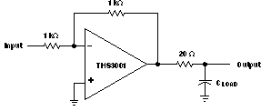
Driving capacitive loads with high-performance amplifiers is not a problem as long as certain precautions are taken. The first is to realize that the THS3001 has been internally compensated to maximize the bandwidth and slew-rate performance. When the amplifier is compensated in this manner, capacitive loading directly on the output decreases the device phase margin leading to high-frequency ringing or oscillations. Therefore, for capacitive loads of greater than 10pF, a resistor needs to be placed in series with the output of the amplifier, as shown in Figure 7-10. A minimum value of 20Ω can work adequately for most applications. For example, in 75Ω transmission systems, setting the series resistor value to 75Ω both isolates any capacitance loading and provides the proper line impedance matching at the source end.
 Figure 7-10 Driving a Capacitive Load