SLOS217I July   1998  – December 2024 THS3001

PRODUCTION DATA  

  1.   1
  2. Features
  3. Applications
  4. Description
  5. Pin Configuration and Functions
  6. Specifications
    1. 5.1 Absolute Maximum Ratings
    2. 5.2 ESD Ratings
    3. 5.3 Recommended Operating Conditions
    4. 5.4 Thermal Information
    5. 5.5 Electrical Characteristics
    6. 5.6 Typical Characteristics
  7. Detailed Description
    1. 6.1 Overview
    2. 6.2 Functional Block Diagram
    3. 6.3 Device Functional Modes
  8. Application and Implementation
    1. 7.1 Application Information
      1. 7.1.1 Recommended Feedback and Gain Resistor Values
      2. 7.1.2 Noise Calculations
      3. 7.1.3 Slew Rate
      4. 7.1.4 Offset Voltage
    2. 7.2 Typical Applications
      1. 7.2.1 General Configurations
      2. 7.2.2 Driving a Capacitive Load
    3. 7.3 Power Supply Recommendations
    4. 7.4 Layout
      1. 7.4.1 Layout Guidelines
        1. 7.4.1.1 PCB Design Considerations
        2. 7.4.1.2 Thermal Considerations
  9. Device and Documentation Support
    1. 8.1 Device Support
      1. 8.1.1 Evaluation Board
    2. 8.2 Receiving Notification of Documentation Updates
    3. 8.3 Support Resources
    4. 8.4 Trademarks
    5. 8.5 Electrostatic Discharge Caution
    6. 8.6 Glossary
  10. Revision History
  11. 10Mechanical, Packaging, and Orderable Information

Package Options

Refer to the PDF data sheet for device specific package drawings

Mechanical Data (Package|Pins)
  • D|8
  • DGN|8
Thermal pad, mechanical data (Package|Pins)
Orderable Information

Thermal Considerations

The THS3001 incorporates output-current-limiting protection. If the output is ever shorted to ground, the output current is automatically limited to the value given in the data sheet. While the output-current-limiting protects the output against excessive current, the device internal power dissipation increases due to the high current and large voltage drop across the output transistors.

CAUTION: Continuous output shorts are not recommended and can damage the device. Additionally, connection of the amplifier output to one of the supply rails (VCC or VEE) is not recommended and can result in device failure. In addition, the THS3001 does not incorporate thermal-shutdown protection. Because of this limitation, pay special attention to the device power dissipation, or failure can result.

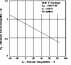
The thermal coefficient θJA is approximately 169°C/W for the SOIC 8-pin D package. For a given θJA, the maximum power dissipation shown in Figure 7-13 is calculated by the following formula:

THS3001
THS3001 Maximum Power Dissipation vs
                    Free-Air Temperature Figure 7-13 Maximum Power Dissipation vs Free-Air Temperature