SLOS217I July 1998 – December 2024 THS3001
PRODUCTION DATA
- 1
- 1 Features
- 2 Applications
- 3 Description
- 4 Pin Configuration and Functions
- 5 Specifications
- 6 Detailed Description
- 7 Application and Implementation
- 8 Device and Documentation Support
- 9 Revision History
- 10Mechanical, Packaging, and Orderable Information
Package Options
Refer to the PDF data sheet for device specific package drawings
Mechanical Data (Package|Pins)
- D|8
- DGN|8
Thermal pad, mechanical data (Package|Pins)
- DGN|8
Orderable Information
7.4.1.1 PCB Design Considerations
Proper PCB design techniques in two areas are important for best performance with the THS3001. These areas are high-speed layout techniques and thermal-management techniques. Because the THS3001 is a high-speed part, the following guidelines are recommended.
- Ground plane: The ground plane needs be used on the board to provide all components with a low inductive ground connection, but needs to be removed from below the output and negative input pins as noted below.
- The DGN package option includes a thermal pad for increased thermal performance. When using this package, the PCB designer needs to distribute the negative supply as a power plane, and tie the thermal pad to this supply with multiple vias for proper power dissipation. Do not tie the thermal pad to ground when using split supply (±V) as this can cause worse distortion performance than shown in this data sheet.
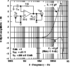
- Input stray capacitance: To minimize potential problems with amplifier oscillation, the capacitance at the inverting input of the amplifiers must be kept to a minimum. To do this, PCB trace runs to the inverting input must be as short as possible, the ground plane must be removed under any etch runs connected to the inverting input, and external components need to be placed as close as possible to the inverting input. This is especially true in the noninverting configuration. An example of this can be seen in Figure 7-11, which shows what happens when a 1pF capacitor is added to the inverting input terminal. The bandwidth increases at the expense of peaking. This is because some of the error current is flowing through the stray capacitor instead of the inverting node of the amplifier. Although, while the device is in the inverting mode, stray capacitance at the inverting input has a minimal effect. This is because the inverting node is at a virtual ground and the voltage does not fluctuate nearly as much as in the noninverting configuration. This can be seen in Figure 7-12, where a 10pF capacitor adds only 0.35dB of peaking. In general, as the gain of the system increases, the output peaking due to this capacitor decreases. While this can initially look like a faster and better system, overshoot and ringing are more likely to occur under fast transient conditions. So proper analysis of adding a capacitor to the inverting input node needs to be performed for stable operation.
 Figure 7-11 Output Amplitude vs
Frequency
 Figure 7-12 Output Amplitude vs
Frequency
Figure 7-12 Output Amplitude vs
Frequency- Proper power-supply decoupling: Use a minimum 6.8μF tantalum capacitor in parallel with a 0.1μF ceramic capacitor on each supply terminal. The tantalum capacitor can be shared among several amplifiers depending on the application, but use a 0.1μF ceramic capacitor on the supply terminal of every amplifier. In addition, place the 0.1μF capacitor as close as possible to the supply terminal. As this distance increases, the inductance in the connecting etch makes the capacitor less effective. In addition, distances of less than 0.1 inch between the device power terminal and the ceramic capacitors are recommended.