SLOS930C November 2015 – October 2024 THS4541-Q1
PRODUCTION DATA
- 1
- 1 Features
- 2 Applications
- 3 Description
- 4 Device Comparison Table
- 5 Pin Configuration and Functions
-
6 Specifications
- 6.1 Absolute Maximum Ratings
- 6.2 ESD Ratings
- 6.3 Recommended Operating Conditions
- 6.4 Thermal Information
- 6.5 Electrical Characteristics: (Vs+) – Vs– = 5 V
- 6.6 Electrical Characteristics: (Vs+) – Vs– = 3 V
- 6.7 Typical Characteristics: 5-V Single Supply
- 6.8 Typical Characteristics: 3-V Single Supply
- 6.9 Typical Characteristics: 3-V to 5-V Supply Range
-
7 Parameter Measurement Information
- 7.1 Example Characterization Circuits
- 7.2 Frequency-Response Shape Factors
- 7.3 I/O Headroom Considerations
- 7.4 Output DC Error and Drift Calculations and the Effect of Resistor Imbalances
- 7.5 Noise Analysis
- 7.6 Factors Influencing Harmonic Distortion
- 7.7 Driving Capacitive Loads
- 7.8 Thermal Analysis
-
8 Detailed Description
- 8.1 Overview
- 8.2 Functional Block Diagram
- 8.3 Feature Description
- 8.4
Device Functional Modes
- 8.4.1
Operation from Single-Ended Sources to Differential Outputs
- 8.4.1.1 AC-Coupled Signal Path Considerations for Single-Ended Input to Differential Output Conversion
- 8.4.1.2 DC-Coupled Input Signal Path Considerations for Single-Ended to Differential Conversion
- 8.4.1.3 Resistor Design Equations for the Single-Ended to Differential Configuration of the FDA
- 8.4.1.4 Input Impedance for the Single-Ended to Differential FDA Configuration
- 8.4.2 Differential-Input to Differential-Output Operation
- 8.4.1
Operation from Single-Ended Sources to Differential Outputs
- 9 Application and Implementation
- 10Device and Documentation Support
- 11Revision History
- 12Mechanical, Packaging, and Orderable Information
Package Options
Refer to the PDF data sheet for device specific package drawings
Mechanical Data (Package|Pins)
- RGT|16
Thermal pad, mechanical data (Package|Pins)
- RGT|16
Orderable Information
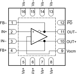
5 Pin Configuration and Functions
 Figure 5-1 RGT Package,
16-Pin VQFN With Exposed Thermal Pad, (Top View)
Figure 5-1 RGT Package,
16-Pin VQFN With Exposed Thermal Pad, (Top View)Table 5-1 Pin Functions
| PIN | TYPE | DESCRIPTION | |
|---|---|---|---|
| NAME | NO.(1) | ||
| FB+ | 4 | Output | Noninverted (positive) output feedback |
| FB– | 1 | Output | Inverted (negative) output feedback |
| IN+ | 2 | Input | Noninverting (positive) amplifier input |
| IN– | 3 | Input | Inverting (negative) amplifier input |
| NC | — | — | No internal connection |
| OUT+ | 10 | Output | Noninverted (positive) amplifier output |
| OUT– | 11 | Output | Inverted (negative) amplifier output |
| PD | 12 | Input | Power down. PD = logic low = power off mode; PD = logic high = normal operation. |
| Vocm | 9 | Input | Common-mode voltage input |
| Vs+ | 5–8 | Input | Positive power-supply input |
| Vs– | 13–16 | Input | Negative power-supply input |
(1) Solder the exposed thermal pad to a
heat-spreading power or ground plane. This pad is
electrically isolated from the die, but must be connected to
a power or ground plane and not floated.