SLOS930C November 2015 – October 2024 THS4541-Q1
PRODUCTION DATA
- 1
- 1 Features
- 2 Applications
- 3 Description
- 4 Device Comparison Table
- 5 Pin Configuration and Functions
-
6 Specifications
- 6.1 Absolute Maximum Ratings
- 6.2 ESD Ratings
- 6.3 Recommended Operating Conditions
- 6.4 Thermal Information
- 6.5 Electrical Characteristics: (Vs+) – Vs– = 5 V
- 6.6 Electrical Characteristics: (Vs+) – Vs– = 3 V
- 6.7 Typical Characteristics: 5-V Single Supply
- 6.8 Typical Characteristics: 3-V Single Supply
- 6.9 Typical Characteristics: 3-V to 5-V Supply Range
-
7 Parameter Measurement Information
- 7.1 Example Characterization Circuits
- 7.2 Frequency-Response Shape Factors
- 7.3 I/O Headroom Considerations
- 7.4 Output DC Error and Drift Calculations and the Effect of Resistor Imbalances
- 7.5 Noise Analysis
- 7.6 Factors Influencing Harmonic Distortion
- 7.7 Driving Capacitive Loads
- 7.8 Thermal Analysis
-
8 Detailed Description
- 8.1 Overview
- 8.2 Functional Block Diagram
- 8.3 Feature Description
- 8.4
Device Functional Modes
- 8.4.1
Operation from Single-Ended Sources to Differential Outputs
- 8.4.1.1 AC-Coupled Signal Path Considerations for Single-Ended Input to Differential Output Conversion
- 8.4.1.2 DC-Coupled Input Signal Path Considerations for Single-Ended to Differential Conversion
- 8.4.1.3 Resistor Design Equations for the Single-Ended to Differential Configuration of the FDA
- 8.4.1.4 Input Impedance for the Single-Ended to Differential FDA Configuration
- 8.4.2 Differential-Input to Differential-Output Operation
- 8.4.1
Operation from Single-Ended Sources to Differential Outputs
- 9 Application and Implementation
- 10Device and Documentation Support
- 11Revision History
- 12Mechanical, Packaging, and Orderable Information
Package Options
Refer to the PDF data sheet for device specific package drawings
Mechanical Data (Package|Pins)
- RGT|16
Thermal pad, mechanical data (Package|Pins)
- RGT|16
Orderable Information
3 Description
The THS4541-Q1 is a low-power, voltage-feedback, fully differential amplifier (FDA) with an input common-mode range less than the negative rail, and rail-to-rail output. Designed for low-power data acquisition systems where high density is critical in a high-performance analog-to-digital converter (ADC) or digital-to-analog converter (DAC) interface design.
The THS4541-Q1 features the negative-rail input required when interfacing a dc-coupled, ground-centered, source signal. This negative-rail input, with rail-to-rail output, allows for an easy interface between single-ended, ground-referenced, bipolar signal sources and a wide variety of successive approximation register (SAR), delta-sigma (ΔΣ), or pipeline ADCs using only a single 2.7V to 5.4V power supply.
The THS4541-Q1 is characterized for operation over the wide temperature range of –40°C to +125°C and is available in a 16-pin VQFN package, both with and without wettable flanks. The package with wettable flanks eases post-assembly visual inspection and is available as the THS4541W-Q1.
| PART NUMBER(1) | PACKAGE(2) | PACKAGE SIZE(3) |
|---|---|---|
| THS4541-Q1 | RGT (VQFN, 16) | 3mm × 3mm |
| THS4541W-Q1(4) |
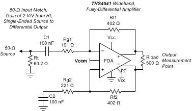
 Simplified
Schematic
 Single to
Differential Gain of 2, 2VPP
Output