SBOS778D April 2016 – April 2021 THS4551
PRODUCTION DATA
- 1 Features
- 2 Applications
- 3 Description
- 4 Revision History
- 5 Companion Devices
- 6 Pin Configuration and Functions
-
7 Specifications
- 7.1 Absolute Maximum Ratings
- 7.2 ESD Ratings
- 7.3 Recommended Operating Conditions
- 7.4 Thermal Information
- 7.5 Electrical Characteristics: (VS+) – (VS–) = 5 V
- 7.6 Electrical Characteristics: (VS+) – (VS–) = 3 V
- 7.7 Typical Characteristics: (VS+) – (VS–) = 5 V
- 7.8 Typical Characteristics: (VS+) – (VS–) = 3 V
- 7.9 Typical Characteristics: 3-V to 5-V Supply Range
-
8 Parameter Measurement Information
- 8.1 Example Characterization Circuits
- 8.2 Output Interface Circuit for DC-Coupled Differential Testing
- 8.3 Output Common-Mode Measurements
- 8.4 Differential Amplifier Noise Measurements
- 8.5 Balanced Split-Supply Versus Single-Supply Characterization
- 8.6 Simulated Characterization Curves
- 8.7 Terminology and Application Assumptions
- 9 Detailed Description
- 10Application and Implementation
- 11Power Supply Recommendations
- 12Layout
- 13Device and Documentation Support
- 14Mechanical, Packaging, and Orderable Information
Package Options
Mechanical Data (Package|Pins)
Thermal pad, mechanical data (Package|Pins)
Orderable Information
13.1.1 TINA-TI Simulation Model Features
The device model is available on the product folder under www.ti.com in a typical application circuit file. The model includes numerous features intended to speed designer progress over a wide range of application requirements. The following list shows the performance parameters included in the model:
- For the small-signal response shape with any external circuit:
- Differential open-loop gain and phase
- Parasitic input capacitance
- Open-loop differential output impedance
- For noise simulations:
- Input differential spot voltage noise and a 100-Hz 1/f corner
- Input current noise on each input with a 6-kHz 1/f corner
- For time-domain, step-response simulations:
- Differential slew rate
- I/O headroom models to predict clipping
- Input stage diodes to predict overdrive limiting
- Fine-scale, dc precision terms:
- PSRR
- CMRR
The Section 7.9 provides more detail than the macromodels can provide; some of the unmodeled features include:
- Harmonic distortion
- Temperature drift in dc error terms (VIO and IOS)
- Overdrive recovery time
- Turn-on and turn-off times using the power-down feature
Some unique simulation considerations come with the THS4551 TINA-TI™ model. This device (and model) include 0.6-pF internal feedback capacitors. These capacitors are intended to improve phase margin when using higher external feedback resistor values. Higher feedback resistors generate an in-band pole in the feedback signal with the differential input capacitance, and the internal 0.6 pF capacitors add a zero to the feedback response shape to shape the noise gain flat at the loop-gain crossover.
In order to generate an accurate open-loop gain and phase simulation, these components must be removed because they are feedback elements, not forward path elements. Figure 13-1 illustrates a typical AOL gain and phase simulation (available as a TINA-TI™ software file) where external –0.6-pF capacitors cancel out the internal capacitors in the model (TINA-TI™ supports negative value elements). The inductors inside the loop close the loop for the dc operating point and open the loop immediately for an ac sweep. The input-coupling capacitors are open at dc, then couple in the differential input immediately on an ac sweep. The somewhat odd values help reduce numerical chatter in the simulation. When using the internal feedback traces from the outputs to the inputs on the RGT package, be sure to add the 3.3-Ω trace impedance to any simulation. This impedance is not included in the core model.
 Figure 13-1 Open-Loop Gain and Phase TINA-TI™ Simulation Setup
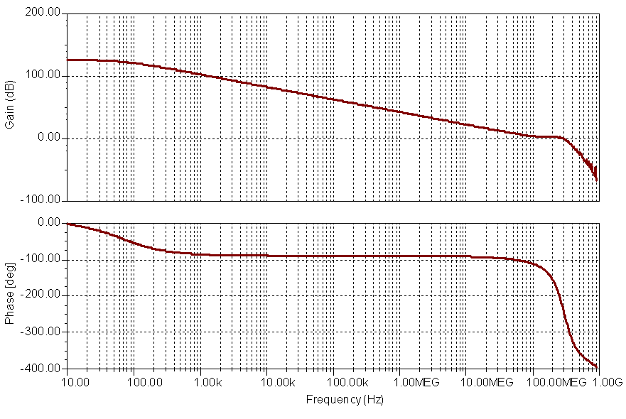
This test is set up with a very light load to isolate the no load AOL curve. Adding a load brings in the open-loop ZOL response to the overall response of the output pins. Running this simulation gives the gain and phase of Figure 13-2 that closely matches the plot of Figure 7-37.
 Figure 13-2 Open-Loop Gain and Phase Simulation Result