At TA = 25 °C, VS pin = 12 V, GND = 0
V, gain = 11 V/V, 100 Ω Load, RSERIES = 47.5
Ω, PAR = 15
dB, and output power measured at input of transformer (1:1) with
no assumed transformer insertion losses (unless otherwise noted).
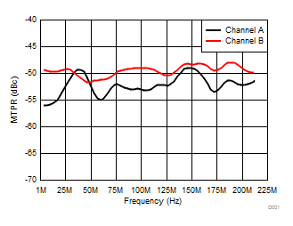 Figure 6-1 MTPR G.Fast 212-MHz Mode
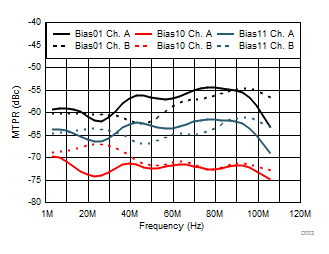 Figure 6-3 MTPR G.Fast 106-MHz Mode
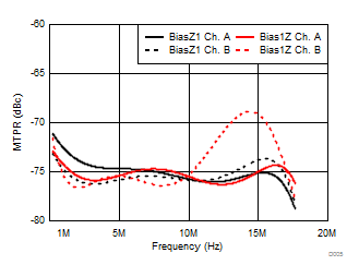 Figure 6-5 MTPR VDSL-17a Mode
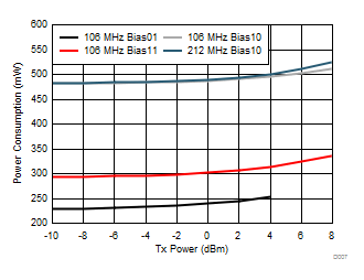 Figure 6-7 G.Fast Modes Power Consumption
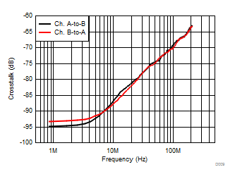 Figure 6-9 Crosstalk G.Fast 212-MHz Mode
| G.Fast 106-MHz channel A, line power =
8 dBm |
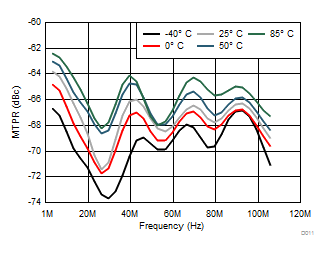
Figure 6-11 MTPR vs Temperature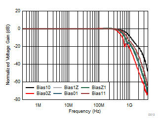 Figure 6-13 Normalized Small-Signal Frequency
Response
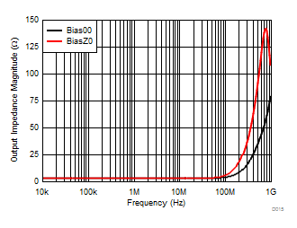 Figure 6-15 Terminal Modes Output Impedance
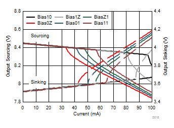
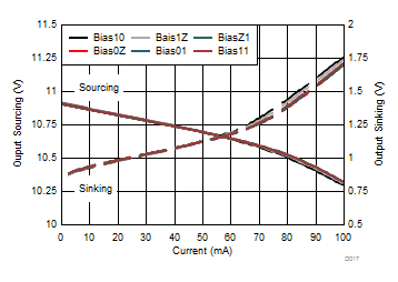 Figure 6-17 Output Voltage vs Current
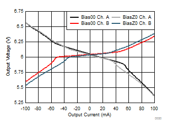
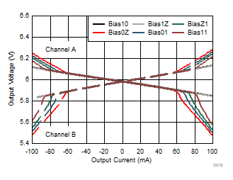 Figure 6-19 Output Voltage vs Current
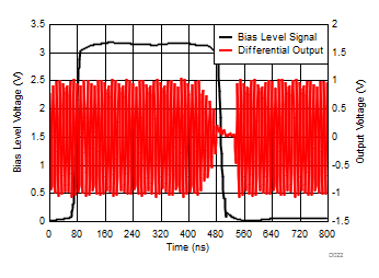
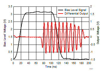 Figure 6-21 Mode Switching Time
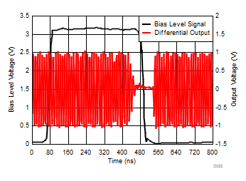 Figure 6-23 Mode Switching Time
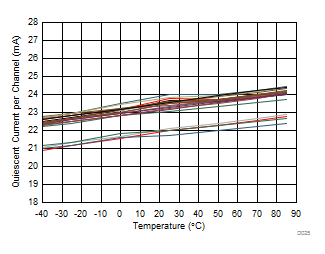
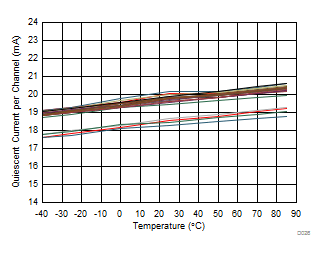
| 10 devices, channels A and B, G.Fast
106-MHz bias (mode 11) |
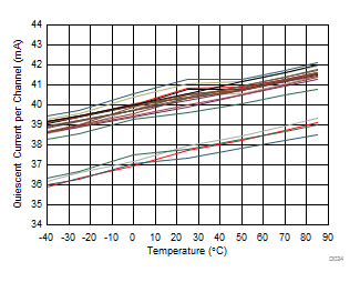
Figure 6-25 Quiescent Current vs Temperature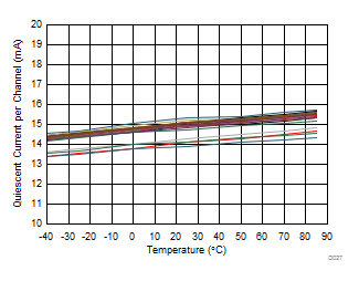
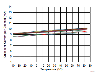
| 10 devices, channels A and B, ADSL bias
(mode 0Z) |
Figure 6-27 Quiescent Current vs Temperature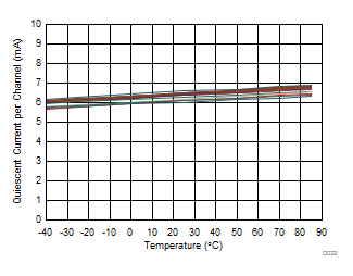
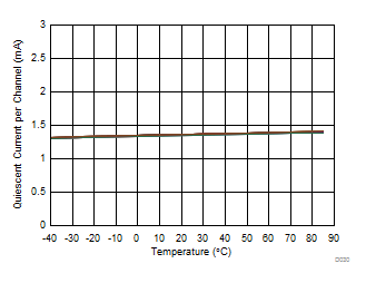
| 10 devices, channels A and B,
line-termination low-power bias (mode Z0) |
Figure 6-29 Quiescent Current vs Temperature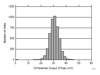 Figure 6-31 Output Offset Voltage
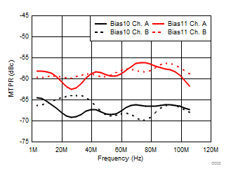 Figure 6-2 MTPR G.Fast 106-MHz Mode
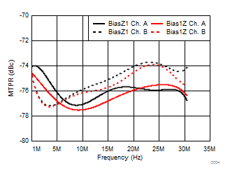 Figure 6-4 MTPR VDSL-30a Mode
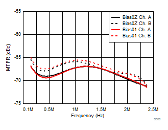 Figure 6-6 MTPR ADSL2+ Mode
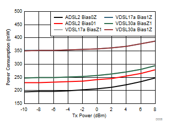 Figure 6-8 xDSL Modes Power Consumption
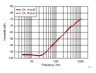 Figure 6-10 Crosstalk G.Fast 106-MHz Mode
| G.Fast 106-MHz channel B, line power =
8 dBm |
Figure 6-12 MTPR vs Temperature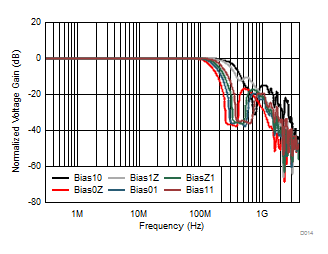 Figure 6-14 Normalized Large-Signal Frequency
Response
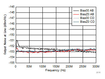 Figure 6-16 Terminal Modes Noise Floor
 Figure 6-18 Output Voltage vs Current
 Figure 6-20 Output Voltage vs Current
 Figure 6-22 Mode Switching Time
| 10 devices, channels A and B, G.Fast
212-MHz bias (mode 10) |
Figure 6-24 Quiescent Current vs Temperature
| 10 devices, channels A and B, VDSL bias
(mode Z1) |
Figure 6-26 Quiescent Current vs Temperature
| 10 devices, channels A and B,
line-termination high-power bias (mode 00) |
Figure 6-28 Quiescent Current vs Temperature
| 10 devices, channels A and B,
power-down (mode ZZ) |
|
Figure 6-30 Quiescent Current vs Temperature


 Figure 6-7 G.Fast Modes Power Consumption
 Figure 6-9 Crosstalk G.Fast 212-MHz Mode
 Figure 6-13 Normalized Small-Signal Frequency
Response
 Figure 6-15 Terminal Modes Output Impedance


 Figure 6-31 Output Offset Voltage


 Figure 6-8 xDSL Modes Power Consumption
 Figure 6-10 Crosstalk G.Fast 106-MHz Mode

 Figure 6-16 Terminal Modes Noise Floor