SBOS746A June 2016 – February 2021 THS6302
PRODUCTION DATA
- 1 Features
- 2 Applications
- 3 Description
- 4 Revision History
- 5 Pin Configuration and Functions
- 6 Specifications
- 7 Detailed Description
- 8 Application and Implementation
- 9 Power Supply Recommendations
- 10Layout
- 11Device and Documentation Support
- 12Mechanical, Packaging, and Orderable Information
Package Options
Mechanical Data (Package|Pins)
- RHF|28
Thermal pad, mechanical data (Package|Pins)
- RHF|28
Orderable Information
7.3 Feature Description
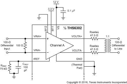
The THS6302 is a dual-channel line driver that has a high current drive and a differential input and output amplifier in each channel. Figure 7-1 shows an example circuit for channel A of the THS6302 configured to drive the G.Fast 212-MHz DSL profile. The bias control pins (M12 and M11) are set to ground and 3.3 V, respectively, to put the device in the G.Fast 212-MHz bias mode. This bias optimizes the internal power consumption of the device to meet performance specifications of the G.Fast 212-MHz profile and can be changed to meet several different DSL profiles and other modes listed in Table 7-1. The IREF pin is biased with a 75-kΩ (RIREF) resistor that adjusts the device quiescent current to a nominal state. RIREF can be increased to lower the quiescent current or deceased to raise the quiescent current of the device for fine-tuning. CIREF provides decoupling for the IREF pin and is typically 100 pF.
The THS6302 has a 10-kΩ, internally-set differential input impedance and low output impedance. In Figure 7-1 the input impedance is matched to 100 Ω by using a 100-Ω resistor connected differentially across the inputs. This value can easily be changed by using a different resistor to create the desired impedance at the input. Remember that the impedance in the device is actually the parallel combination of 10 kΩ and the external input resistor. For low impedances, this effect is minimal, but must be considered if the matched input impedance is increased. The output impedance of the THS6302 in Figure 7-1 is set by the two RSERIES resistors to match 100 Ω. The internal output resistance is very low (< 2 Ω per output), so the output impedance is primarily set by the RSERIES resistors. These resistors can be adjusted to match various output impedance values.
 Figure 7-1 G.Fast 212-MHz Driving Mode Example Circuit