SLLSEY3E May   2018  – May 2019 THVD1410 , THVD1450 , THVD1451 , THVD1452

PRODUCTION DATA.  

  1. Features
  2. Applications
  3. Description
    1.     Device Images
      1.      THVD1410 and THVD1450 Simplified Schematic
      2.      THVD1451 Simplified Schematic
      3.      THVD1452 Simplified Schematic
  4. Revision History
  5. Device Comparison Table
  6. Pin Configuration and Functions
    1.     Pin Functions
    2.     Pin Functions
    3.     Pin Functions
  7. Specifications
    1. 7.1  Absolute Maximum Ratings
    2. 7.2  ESD Ratings
    3. 7.3  ESD Ratings [IEC]
    4. 7.4  Recommended Operating Conditions
    5. 7.5  Thermal Information
    6. 7.6  Power Dissipation
    7. 7.7  Electrical Characteristics
    8. 7.8  Switching Characteristics
    9. 7.9  Typical Characteristics: All Devices
    10. 7.10 Typical Characteristics: THD1450, THVD1451 and THVD1452
    11. 7.11 Typical Characteristics: THVD1410
  8. Parameter Measurement Information
  9. Detailed Description
    1. 9.1 Overview
    2. 9.2 Functional Block Diagrams
    3. 9.3 Feature Description
    4. 9.4 Device Functional Modes
      1. 9.4.1 Device Functional Modes for THVD1410 and THVD1450
      2. 9.4.2 Device Functional Modes for THVD1451
      3. 9.4.3 Device Functional Modes for THVD1452
  10. 10Application and Implementation
    1. 10.1 Application Information
    2. 10.2 Typical Application
      1. 10.2.1 Design Requirements
        1. 10.2.1.1 Data Rate and Bus Length
        2. 10.2.1.2 Stub Length
        3. 10.2.1.3 Bus Loading
        4. 10.2.1.4 Receiver Failsafe
        5. 10.2.1.5 Transient Protection
      2. 10.2.2 Detailed Design Procedure
      3. 10.2.3 Application Curves
  11. 11Power Supply Recommendations
  12. 12Layout
    1. 12.1 Layout Guidelines
    2. 12.2 Layout Example
  13. 13Device and Documentation Support
    1. 13.1 Device Support
    2. 13.2 Third-Party Products Disclaimer
    3. 13.3 Related Links
    4. 13.4 Receiving Notification of Documentation Updates
    5. 13.5 Community Resources
    6. 13.6 Trademarks
    7. 13.7 Electrostatic Discharge Caution
    8. 13.8 Glossary
  14. 14Mechanical, Packaging, and Orderable Information

Package Options

Refer to the PDF data sheet for device specific package drawings

Mechanical Data (Package|Pins)
  • D|8
  • DRB|8
Thermal pad, mechanical data (Package|Pins)
Orderable Information

Typical Characteristics: All Devices

THVD1410 THVD1450 THVD1451 THVD1452 D001_SLLSEY3.gif
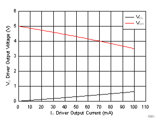
VCC = 5 V DE = VCC D = 0 V
Figure 1. Driver Output Voltage vs Driver Output Current
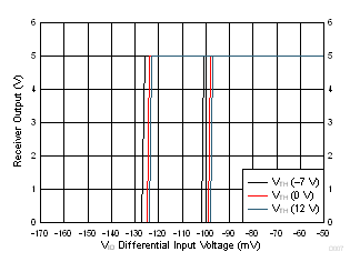
THVD1410 THVD1450 THVD1451 THVD1452 D007_SLLSEY3.gif
VCC = 5 V TA = 25°C
Figure 3. Receiver Output vs Input
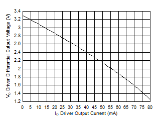
THVD1410 THVD1450 THVD1451 THVD1452 D102_SLLSEY3.gif
VCC = 3.3 V DE = VCC D = 0 V
Figure 5. Driver Differential Output Voltage vs Driver Output Current
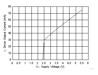
THVD1410 THVD1450 THVD1451 THVD1452 D003_SLLSEY3.gif
TA = 25°C DE = VCC D = VCC
RL = 54 Ω
Figure 7. Driver Output Current vs Supply Voltage
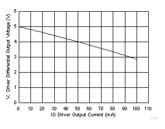
THVD1410 THVD1450 THVD1451 THVD1452 D002_SLLSEY3.gif
VCC = 5 V DE = VCC D = 0 V
Figure 2. Driver Differential Output voltage vs Driver Output Current
THVD1410 THVD1450 THVD1451 THVD1452 D101_SLLSEY3.gif
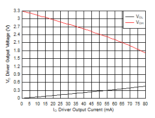
VCC = 3.3 V DE = VCC D = 0 V
Figure 4. Driver Output Voltage vs Driver Output Current
THVD1410 THVD1450 THVD1451 THVD1452 D106_SLLSEY3.gif
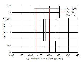
VCC = 3.3 V TA = 25°C
Figure 6. Receiver Output vs Input