SLVS062N December 1991 – October 2016 TL1431 , TL1431M
PRODUCTION DATA.
- 1 Features
- 2 Applications
- 3 Description
- 4 Revision History
- 5 Pin Configuration and Functions
- 6 Specifications
- 7 Parameter Measurement Information
- 8 Detailed Description
- 9 Application and Implementation
- 10Power Supply Recommendations
- 11Layout
- 12Device and Documentation Support
- 13Mechanical, Packaging, and Orderable Information
Package Options
Mechanical Data (Package|Pins)
Thermal pad, mechanical data (Package|Pins)
Orderable Information
9 Application and Implementation
NOTE
Information in the following applications sections is not part of the TI component specification, and TI does not warrant its accuracy or completeness. TI’s customers are responsible for determining suitability of components for their purposes. Customers should validate and test their design implementation to confirm system functionality.
9.1 Application Information
As the TL1431 device has many applications and setups, there are many situations that this datasheet cannot characterize in detail. The linked application notes help the designer make the best choices when using this part. Understanding Stability Boundary Conditions Charts in TL431, TL432 Data Sheet (SLVA482) provides a deeper understanding of this devices stability characteristics and aid the user in making the right choices when choosing a load capacitor. Setting the Shunt Voltage on an Adjustable Shunt Regulator (SLVA445) assists designers in setting the shunt voltage to achieve optimum accuracy for this device.
9.2 Typical Application
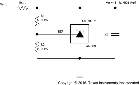 Figure 23. Comparator Application Schematic
9.2.1 Design Requirements
For this design example, use the parameters listed in Table 2 as the input parameters.
Table 2. Design Parameters
| PARAMETER | VALUE |
|---|---|
| Reference initial accuracy | 0.4% |
| Supply voltage | 48 V |
| Cathode current (IK) | 50 µA |
| Output voltage level | 2.5 V to 36 V |
| Load capacitance | 1 nF |
| Feedback resistor values and accuracy (R1 and R2) | 10 kΩ |
9.2.2 Detailed Design Procedure
When using TL1431 as a shunt regulator, determine the following:
- Input voltage range
- Temperature range
- Total accuracy
- Cathode current
- Reference initial accuracy
- Output capacitance
9.2.2.1 Programming Output/Cathode Voltage
To program the cathode voltage to a regulated voltage a resistive bridge must be shunted between the cathode and anode pins with the mid point tied to the reference pin. This can be seen in Figure 23, with R1 and R2 being the resistive bridge. The cathode/output voltage in the shunt regulator configuration can be approximated by the equation shown in Figure 23. The cathode voltage can be more accurately determined by taking in to account the cathode current with Equation 1.
For this equation to be valid, TL1431 must be fully biased so that it has enough open loop gain to mitigate any gain error. This can be done by meeting the Imin specification denoted in Electrical Characteristics – TL1431M.
9.2.2.2 Total Accuracy
When programming the output above unity gain (VKA=VREF), TL1431 is susceptible to other errors that may effect the overall accuracy beyond VREF. These errors include:
- R1 and R2 accuracies
- VI(dev) – Change in reference voltage over temperature
- ΔVREF / ΔVKA – Change in reference voltage to the change in cathode voltage
- |zKA| – Dynamic impedance, causing a change in cathode voltage with cathode current
Worst case cathode voltage can be determined taking all of the variables in to account.
9.2.2.3 Stability
Though TL1431 is stable with no capacitive load, the device that receives the shunt regulator's output voltage could present a capacitive load that is within the TL1431 region of stability, shown in Figure 12. Also, designers may use capacitive loads to improve the transient response or for power supply decoupling. When using additional capacitance between Cathode and Anode, refer to Figure 12.
9.2.2.4 Start-up Time
As shown in Figure 24, TL1431 has a fast response up to approximately 2 V and then slowly charges to its programmed value. This is due to the compensation capacitance the TL1431 has to meet its stability criteria. Despite the secondary delay, TL1431 still has a fast response suitable for many clamp applications.
9.2.3 Application Curve
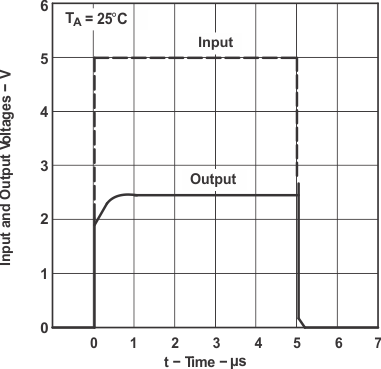 Figure 24. TL1431 Start-up Response
9.3 System Examples
Table 3 lists example circuits of the TL1431.
Table 3. Table Of Example Circuits
| APPLICATION | FIGURE |
|---|---|
| Shunt regulator | Figure 25 |
| Single-supply comparator with temperature-compensated threshold | Figure 26 |
| Precision high-current series regulator | Figure 27 |
| Output control of a three-terminal fixed regulator | Figure 28 |
| Higher-current shunt regulator | Figure 29 |
| Crowbar | Figure 30 |
| Precision 5-V, 1.5-A, 0.5% regulator | Figure 31 |
| 5-V precision regulator | Figure 32 |
| PWM converter with 0.5% reference | Figure 33 |
| Voltage monitor | Figure 34 |
| Delay timer | Figure 35 |
| Precision current limiter | Figure 36 |
| Precision constant-current sink | Figure 37 |
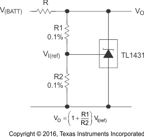
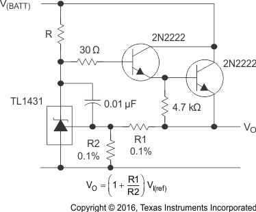
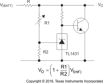 Figure 29. Higher-Current Shunt Regulator
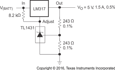 Figure 31. Precision 5-V, 1.5-A, 0.5% Regulator
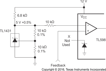 Figure 33. PWM Converter With 0.5% Reference
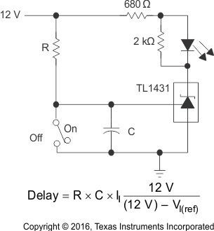 Figure 35. Delay Timer
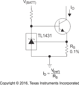 Figure 37. Precision Constant-Current Sink
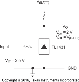 Figure 26. Single-Supply Comparator
 With Temperature-Compensated Threshold
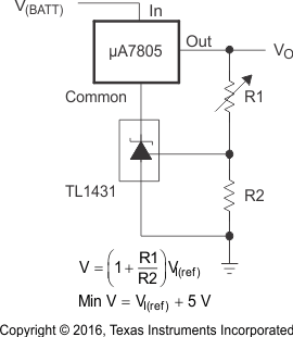 Figure 28. Output Control Of A
 Three-Terminal Fixed Regulator
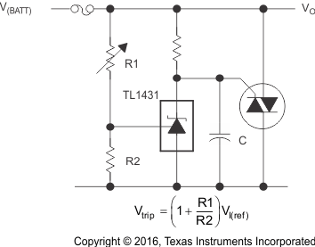
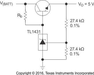
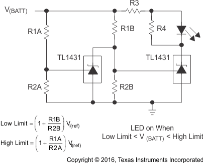
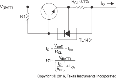 Figure 36. Precision Current Limiter