-
TL499A Wide-Range Power-Supply Controllers
- 1 Features
- 2 Applications
- 3 Description
- 4 Revision History
- 5 Pin Configuration and Functions
- 6 Specifications
- 7 Detailed Description
- 8 Application and Implementation
- 9 Power Supply Recommendations
- 10Layout
- 11Device and Documentation Support
- 12Mechanical, Packaging, and Orderable Information
- IMPORTANT NOTICE
Package Options
Refer to the PDF data sheet for device specific package drawings
Mechanical Data (Package|Pins)
- P|8
- PS|8
Thermal pad, mechanical data (Package|Pins)
Orderable Information
TL499A Wide-Range Power-Supply Controllers
1 Features
2 Applications
- Voltage Boosting
- Dual-Supply Voltage Reglation
- Battery Back-Ups
- Microprocessor Memory Power
3 Description
The TL499A device is an integrated circuit designed to provide a wide range of adjustable regulated supply voltages. The regulated output voltage can be varied from 2.9 V to 30 V by adjusting two external resistors. When the TL499A is ac-coupled to line power through a step-down transformer, it operates as a series DC voltage regulator to maintain the regulated output voltage. With the addition of a battery from 1.1 V to 10 V, an inductor, a filter capacitor, and two resistors, the TL499A operates as a step-up switching regulator during an AC-line failure. The adjustable regulated output voltage makes the TL499A useful for a wide range of applications. Providing backup power during an AC-line failure makes the TL499A extremely useful in microprocessor memory applications. The TL499AC is characterized for operation from –20°C to +85°C.
Device Information(1)
| PART NUMBER | PACKAGE (PIN) | BODY SIZE (NOM) |
|---|---|---|
| TL499A | SO (8) | 6.20 mm × 5.30 mm |
| PDIP (8) | 9.81 mm × 6.35 mm |
- For all available packages, see the orderable addendum at the end of the data sheet.
Typical Application
4 Revision History
Changes from G Revision (September 2001) to H Revision
- Added Pin Configuration and Functions section, ESD Ratings table, Feature Description section, Device Functional Modes, Application and Implementation section, Power Supply Recommendations section, Layout section, Device and Documentation Support section, and Mechanical, Packaging, and Orderable Information section Go
5 Pin Configuration and Functions

Pin Functions
| PIN | I/O | DESCRIPTION | |
|---|---|---|---|
| NAME | NO. | ||
| GND | 5 | — | Signal ground. |
| GND (PWR) | 7 | — | Power ground. |
| OUTPUT | 8 | O | Regulated output |
| REF | 2 | I | Feedback tap for output voltage |
| SERIES IN1 | 1 | — | Power source for series voltage regulator. |
| SW CURRENT CTRL | 4 | I/O | Resistor to ground controls switching current |
| SW IN | 6 | I/O | Step up switching inductor node |
| SW REG IN2 | 3 | — | Power source for step-up switching regulator. |
6 Specifications
6.1 Absolute Maximum Ratings
over operating free-air temperature range (unless otherwise noted)(1)| MIN | MAX | UNIT | |||
|---|---|---|---|---|---|
| VO | Output voltage(2) | –0.3 | 35 | V | |
| VI1 | Input voltage, series regulator | –0.3 | 35 | V | |
| VI2 | Input voltage, switching regulator | –0.3 | 10 | V | |
| Blocking-diode reverse voltage | 35 | V | |||
| Blocking-diode forward current | 1 | A | |||
| SW IN | Power switch current | 1 | A | ||
| Lead temperature 1.6 mm (1/16 inch) from case for 10 seconds | 260 | °C | |||
| TJ | Junction temperature | 150 | °C | ||
| Tstg | Storage temperature | –65 | 150 | °C | |
6.2 ESD Ratings
| VALUE | UNIT | |||
|---|---|---|---|---|
| V(ESD) | Electrostatic discharge | Human body model (HBM), per ANSI/ESDA/JEDEC JS-001(1) | ±200 | V |
| Charged-device model (CDM), per JEDEC specification JESD22-C101(2) | ±2000 | |||
6.3 Recommended Operating Conditions
over operating free-air temperature range (unless otherwise noted)| MIN | NOM | MAX | UNIT | ||
|---|---|---|---|---|---|
| Output voltage, VO | 2.9 | 30 | V | ||
| Input voltage, VI1 (SERIES IN1) | 4.5 | 32 | V | ||
| Input voltage, VI2 (SW REG IN2) | 1.1 | 10 | V | ||
| Output-to-input differential voltage, switching regulator, VO – VI2 (see (1)) | 1.2 | 28.9 | V | ||
| Continuous output current, IO | 100 | mA | |||
| Power switch current (at SW IN) | 500 | mA | |||
| Current-limiting resistor, RCL | 150 | 1000 | Ω | ||
| Filter capacitor | 100 | 470 | µF | ||
| Pass capacitor | 0.1 | µF | |||
| Inductor, L (dcr ≤ 0.1 Ω) | 50 | 150 | µH | ||
| Operating free-air temperature, TA | –20 | 85 | °C | ||
6.4 Thermal Information
| THERMAL METRIC(1) | TL499A | UNIT | ||
|---|---|---|---|---|
| P (PDIP) | PS (SO) | |||
| 8 PINS | 8 PINS | |||
| RθJA | Junction-to-ambient thermal resistance(2)(3) | 49.7 | 110.7 | °C/W |
| RθJC(top) | Junction-to-case (top) thermal resistance | 38.8 | 69.0 | °C/W |
| RθJB | Junction-to-board thermal resistance | 26.9 | 55.7 | °C/W |
| ψJT | Junction-to-top characterization parameter | 16.1 | 20.1 | °C/W |
| ψJB | Junction-to-board characterization parameter | 26.7 | 54.9 | °C/W |
6.5 Electrical Characteristics
over operating free-air temperature range (unless otherwise noted)| PARAMETER | TEST CONDITIONS | MIN | TYP | MAX | UNIT | |
|---|---|---|---|---|---|---|
| Voltage deviation (see (1)) | 20 | 30 | mV/V | |||
| VO – VI2 | Switching regulator minimum boost | TA = –20°C to 70°C | 1.2 | V | ||
| TA = –20°C to 85°C | 1.9 | |||||
| Dropout voltage | Series regulator | VI1 = 15 V, IO = 50 mA | 1.8 | V | ||
| Reference voltage (internal) | VI1 = 5 V, VO = 3 V, IO = 1 mA | 1.2 | 1.26 | 1.32 | V | |
| Reference-voltage change with temperature | 5 | 10 | mV/V | |||
| Output regulation (of reference voltage) | IO = 1 mA to 50 mA | 10 | 30 | mV/V | ||
| Output current (see Figure 3) |
Switching regulator | VI2 = 1.1 V, VO = 12 V, RCL = 150 Ω, TA = 25°C |
10 | mA | ||
| VI2 = 1.5 V, VO = 15 V, RCL = 150 Ω, TA = 25°C |
15 | |||||
| VI2 = 6 V, VO = 30 V, RCL = 150 Ω, TA = 25°C |
65 | |||||
| Series regulator | 100 | |||||
| Standby current | Switching regulator | VI2 = 3 V, VO = 9 V, TA = 25°C | 15 | 80 | µA | |
| Series regulator | VI1 = 15 V, VO = 9 V, RE2 = 4.7 kΩ | 0.8 | 1.2 | mA | ||
6.6 Typical Characteristics
7 Detailed Description
7.1 Overview
The TL499A provides an adjustable output voltage between 2.9 V and 30 V. The primary power source uses the internal linear regulator to provide the output voltage. When the primary power source is removed, the secondary power source is stepped up using the internal switching regulator to provide the output voltage.
7.2 Functional Block Diagram

7.3 Feature Description
The TL499A has an adjustable output voltage set by feedback provided to REF pin abs an adjustable switching current is set by value of resistor on SW CURRENT CONTROL pin. The lower resistance provides increased switching current.
Dual power supply inputs also provide protection against power faults on the main supply of the TL499A.
7.4 Device Functional Modes
The TL499A has two functional modes:
- Linear voltage regulation when SERIES IN1 supply is present.
- Step-up voltage regulation when SERIES IN1 supply is absent.
8 Application and Implementation
NOTE
Information in the following applications sections is not part of the TI component specification, and TI does not warrant its accuracy or completeness. TI’s customers are responsible for determining suitability of components for their purposes. Customers should validate and test their design implementation to confirm system functionality.
8.1 Application Information
One or two power sources will be regulated to an output voltage set by two feedback resistors.
8.2 Typical Application
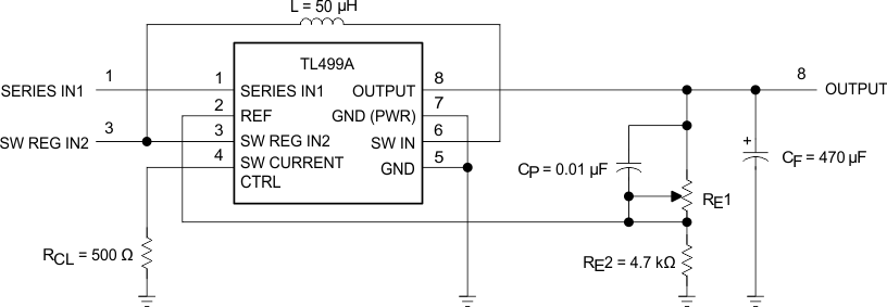
Figure 3 shows the basic configuration of the two power source voltage regulator
 Figure 3. TL499A Basic Configuration
8.2.1 Design Requirements
Provide one or more of the following power sources:
- SERIES IN1 voltage greater than OUTPUT voltage by more than dropout voltage
- SW REG IN2 voltage less than OUTPUT voltage
Select RCL value based on Table 1 through Table 5.
Table 1. Maximum Output Current vs Input and Output Voltages for Step-Up Switching Regulator With RCL = 150 Ω
| OUTPUT VOLTAGE (V) | SWITCHING REGULATOR INPUT VOLTAGE (SW REG IN2) (V) | ||||||||||||
|---|---|---|---|---|---|---|---|---|---|---|---|---|---|
| 1.1 | 1.2 | 1.3 | 1.5 | 1.7 | 2 | 2.5 | 3 | 5 | 6 | 9 | |||
| OUTPUT CURRENT (mA) | |||||||||||||
| 30 | 65 | 90 | |||||||||||
| 25 | 50 | 80 | 100 | ||||||||||
| 20 | 20 | 25 | 30 | 85 | 100 | 100 | |||||||
| 15 | 15 | 20 | 30 | 45 | 55 | 100 | 100 | 100 | |||||
| 12 | 10 | 15 | 20 | 25 | 30 | 40 | 55 | 70 | 100 | 100 | 100 | ||
| 10 | 15 | 20 | 25 | 30 | 35 | 45 | 65 | 80 | 100 | 100 | |||
| 9 | 20 | 25 | 25 | 35 | 40 | 50 | 70 | 90 | 100 | 100 | |||
| 6 | 30 | 35 | 40 | 45 | 55 | 75 | 95 | 100 | |||||
| 5 | 35 | 40 | 45 | 55 | 70 | 85 | 100 | 100 | Circuit of Figure 1, except: RCL = 150 Ω CF = 330 μF CP = 0.1 μF |
||||
| 4.5 | 35 | 45 | 50 | 60 | 75 | 95 | 100 | 100(1) | |||||
| 3 | 55 | 65(1) | 75(1) | 95(1) | 100(1) | ||||||||
| 2.9 | 60(1) | 70(1) | 75(1) | 100(1) | 100(1) | ||||||||
Table 2. Maximum Output Current vs Input and Output Voltages for Step-Up Switching Regulator With RCL = 200 Ω
| OUTPUT VOLTAGE (V) | SWITCHING REGULATOR INPUT VOLTAGE (SW REG IN2) (V) | ||||||||||||
|---|---|---|---|---|---|---|---|---|---|---|---|---|---|
| 1.1 | 1.2 | 1.3 | 1.5 | 1.7 | 2 | 2.5 | 3 | 5 | 6 | 9 | |||
| OUTPUT CURRENT (mA) | |||||||||||||
| 30 | 50 | 100 | |||||||||||
| 25 | 50 | 70 | 100 | ||||||||||
| 20 | 15 | 25 | 30 | 70 | 90 | 100 | |||||||
| 15 | 10 | 15 | 25 | 35 | 45 | 90 | 100 | 100 | |||||
| 12 | 10 | 10 | 15 | 20 | 25 | 35 | 45 | 60 | 100 | 100 | 100 | ||
| 10 | 15 | 20 | 20 | 25 | 30 | 40 | 55 | 70 | 100 | 100 | |||
| 9 | 20 | 20 | 25 | 30 | 35 | 45 | 60 | 80 | 100 | ||||
| 6 | 25 | 30 | 35 | 45 | 50 | 65 | 90 | 100 | |||||
| 5 | 30 | 35 | 40 | 55 | 60 | 75 | 100 | 100 | Circuit of Figure 1, except: RCL = 200 Ω CF = 330 μF CP = 0.1 μF |
||||
| 4.5 | 35 | 40 | 45 | 55 | 65 | 85 | 100 | 100(1) | |||||
| 3 | 50 | 55(1) | 65(1) | 80(1) | 90(1) | ||||||||
| 2.9 | 50(1) | 60(1) | 65(1) | 85(1) | 100(1) | ||||||||
Table 3. Maximum Output Current vs Input and Output Voltages for Step-Up Switching Regulator With RCL = 300 Ω
| OUTPUT VOLTAGE (V) | SWITCHING REGULATOR INPUT VOLTAGE (SW REG IN2) (V) | ||||||||||||
|---|---|---|---|---|---|---|---|---|---|---|---|---|---|
| 1.1 | 1.2 | 1.3 | 1.5 | 1.7 | 2 | 2.5 | 3 | 5 | 6 | 9 | |||
| OUTPUT CURRENT (mA) | |||||||||||||
| 30 | 40 | 70 | |||||||||||
| 25 | 40 | 55 | 100 | ||||||||||
| 20 | 10 | 15 | 20 | 55 | 70 | 100 | |||||||
| 15 | 10 | 10 | 20 | 30 | 35 | 75 | 95 | 100 | |||||
| 12 | 10 | 10 | 10 | 15 | 20 | 25 | 35 | 45 | 95 | 100 | 100 | ||
| 10 | 15 | 15 | 15 | 20 | 25 | 30 | 45 | 55 | 100 | 100 | |||
| 9 | 15 | 15 | 20 | 25 | 30 | 35 | 50 | 60 | 100 | 100 | |||
| 6 | 25 | 25 | 30 | 35 | 45 | 55 | 70 | 90 | |||||
| 5 | 30 | 30 | 35 | 45 | 50 | 65 | 85 | 100 | Circuit of Figure 1, except: RCL = 300 Ω CF = 330 μF CP = 0.1 μF |
||||
| 4.5 | 30 | 35 | 40 | 45 | 55 | 70 | 95 | 100(1) | |||||
| 3 | 45 | 50(1) | 55(1) | 70(1) | 90(1) | ||||||||
| 2.9 | 45(1) | 50(1) | 60(1) | 75(1) | 95(1) | ||||||||
Table 4. Maximum Output Current vs Input and Output Voltages for Step-Up Switching Regulator With RCL = 510 Ω
| OUTPUT VOLTAGE (V) | SWITCHING REGULATOR INPUT VOLTAGE (SW REG IN2) (V) | ||||||||||||
|---|---|---|---|---|---|---|---|---|---|---|---|---|---|
| 1.1 | 1.2 | 1.3 | 1.5 | 1.7 | 2 | 2.5 | 3 | 5 | 6 | 9 | |||
| OUTPUT CURRENT (mA) | |||||||||||||
| 30 | 30 | 50 | |||||||||||
| 25 | 25 | 40 | 75 | ||||||||||
| 20 | 40 | 55 | 90 | ||||||||||
| 15 | 15 | 20 | 55 | 70 | 100 | ||||||||
| 12 | 10 | 15 | 25 | 35 | 65 | 80 | 100 | ||||||
| 10 | 10 | 20 | 25 | 30 | 40 | 70 | 85 | ||||||
| 9 | 10 | 10 | 10 | 15 | 20 | 25 | 35 | 45 | 75 | 100 | |||
| 6 | 15 | 20 | 20 | 25 | 30 | 35 | 50 | 60 | |||||
| 5 | 20 | 20 | 35 | 30 | 35 | 45 | 55 | 70 | Circuit of Figure 1, except: RCL = 510 Ω CF = 330 μF CP = 0.1 μF |
||||
| 4.5 | 25 | 25 | 30 | 35 | 40 | 50 | 65 | 90(1) | |||||
| 3 | 35 | 35(1) | 40(1) | 50(1) | 75(1) | ||||||||
| 2.9 | 35(1) | 35(1) | 40(1) | 55(1) | 80(1) | ||||||||
Table 5. Maximum Output Current vs Input and Output Voltages for Step-Up Switching Regulator With RCL = 1 kΩ
| OUTPUT VOLTAGE (V) | SWITCHING REGULATOR INPUT VOLTAGE (SW REG IN2) (V) | ||||||||||||
|---|---|---|---|---|---|---|---|---|---|---|---|---|---|
| 1.1 | 1.2 | 1.3 | 1.5 | 1.7 | 2 | 2.5 | 3 | 5 | 6 | 9 | |||
| OUTPUT CURRENT (mA) | |||||||||||||
| 30 | 35 | ||||||||||||
| 25 | 35 | 50 | |||||||||||
| 20 | 35 | 60 | |||||||||||
| 15 | 10 | 30 | 45 | 65 | |||||||||
| 12 | 20 | 40 | 45 | 85 | |||||||||
| 10 | 15 | 25 | 40 | 55 | |||||||||
| 9 | 10 | 10 | 15 | 25 | 30 | 45 | 60 | ||||||
| 6 | 10 | 10 | 10 | 15 | 20 | 20 | 30 | 35 | |||||
| 5 | 10 | 10 | 15 | 20 | 20 | 25 | 35 | 40 | Circuit of Figure 1, except: RCL = 1 kΩ CF = 330 μF CP = 0.1 μF |
||||
| 4.5 | 15 | 15 | 15 | 20 | 25 | 30 | 40 | 45(1) | |||||
| 3 | 20 | 25(1) | 25(1) | 30(1) | 35(1) | ||||||||
| 2.9 | 20(1) | 25(1) | 25(1) | 30(1) | 45(1) | ||||||||
8.2.2 Detailed Design Procedure
Select the values for RE1and RE2 using Equation 1:
8.2.3 Application Curve
| IOUT = 50 mA |