SLVS052I April 1988 – September 2016 TL594
PRODUCTION DATA.
- 1 Features
- 2 Applications
- 3 Description
- 4 Revision History
- 5 Pin Configuration and Functions
- 6 Specifications
- 7 Parameter Measurement Information
- 8 Detailed Description
-
9 Application and Implementation
- 9.1 Application Information
- 9.2 Typical Application
- 10Power Supply Recommendations
- 11Layout
- 12Device and Documentation Support
- 13Mechanical, Packaging, and Orderable Information
Package Options
Refer to the PDF data sheet for device specific package drawings
Mechanical Data (Package|Pins)
- PW|16
- NS|16
- N|16
- D|16
Thermal pad, mechanical data (Package|Pins)
Orderable Information
6 Specifications
6.1 Absolute Maximum Ratings
over operating free-air temperature range (unless otherwise noted)(1)| MIN | MAX | UNIT | ||
|---|---|---|---|---|
| Supply voltage, VCC(2) | 41 | V | ||
| Amplifier input voltage | VCC + 0.3 | V | ||
| Collector output voltage | 41 | V | ||
| Collector output current | 250 | mA | ||
| Operating junction temperature, TJ | 150 | °C | ||
| Storage temperature, Tstg | –65 | 150 | °C | |
(1) Stresses beyond those listed under Absolute Maximum Ratings may cause permanent damage to the device. These are stress ratings only, which do not imply functional operation of the device at these or any other conditions beyond those indicated under Recommended Operating Conditions. Exposure to absolute-maximum-rated conditions for extended periods may affect device reliability.
(2) All voltage values, except differential voltages, are with respect to the network ground terminal.
6.2 ESD Ratings
| VALUE | UNIT | |||
|---|---|---|---|---|
| V(ESD) | Electrostatic discharge | Human-body model (HBM), per ANSI/ESDA/JEDEC JS-001(1) | 1000 | V |
| Charged-device model (CDM), per JEDEC specification JESD22-C101(2) | 1000 | |||
(1) JEDEC document JEP155 states that 500-V HBM allows safe manufacturing with a standard ESD control process.
(2) JEDEC document JEP157 states that 250-V CDM allows safe manufacturing with a standard ESD control process.
6.3 Recommended Operating Conditions
| MIN | MAX | UNIT | |||
|---|---|---|---|---|---|
| VCC | Supply voltage | 7 | 40 | V | |
| VI | Amplifier input voltage | –0.3 | VCC – 2 | V | |
| VO | Collector output voltage | 40 | V | ||
| Collector output current (each transistor) | 200 | mA | |||
| Current into FEEDBACK terminal | 0.3 | mA | |||
| CT | Timing capacitor | 0.47 | 10000 | nF | |
| RT | Timing resistor | 1.8 | 500 | kΩ | |
| fosc | Oscillator frequency | 1 | 300 | kHz | |
| TA | Operating free-air temperature | TL594C | 0 | 70 | °C |
| TL594I | –40 | 85 | |||
6.4 Thermal Information
| THERMAL METRIC(1) | TL594 | UNIT | ||||
|---|---|---|---|---|---|---|
| D (SOIC) | N (PDIP) | NS (SO) | PW (TSSOP) | |||
| 16 PINS | 16 PINS | 16 PINS | 16 PINS | |||
| RθJA | Junction-to-ambient thermal resistance | 73.5 | 43.5 | 73.6 | 101.5 | °C/W |
| RθJC(top) | Junction-to-case (top) thermal resistance | 32.8 | 30.6 | 30.3 | 29.4 | °C/W |
| RθJB | Junction-to-board thermal resistance | 30.8 | 23.5 | 34.4 | 47.3 | °C/W |
| ψJT | Junction-to-top characterization parameter | 6.1 | 15.3 | 3.4 | 1.4 | °C/W |
| ψJB | Junction-to-board characterization parameter | 30.6 | 23.4 | 34.1 | 46.6 | °C/W |
(1) For more information about traditional and new thermal metrics, see the Semiconductor and IC Package Thermal Metrics application report.
6.5 Electrical Characteristics
VCC = 15 V, over recommended operating free-air temperature range (unless otherwise noted)| PARAMETER | TEST CONDITIONS(1) | MIN | TYP(2) | MAX | UNIT | |
|---|---|---|---|---|---|---|
| REFERENCE | ||||||
| Output voltage (REF) | IO = 1 mA, TA = 25°C | 4.95 | 5 | 5.05 | V | |
| Input regulation | VCC = 7 V to 40 V, TA = 25°C | 2 | 25 | mV | ||
| Output regulation | IO = 1 mA to 10 mA, TA = 25°C | 14 | 35 | mV | ||
| Output-voltage change with temperature | ΔTA = MIN to MAX | 2 | 10 | mV/V | ||
| Short-circuit output current(3) | Vref = 0 | 10 | 35 | 50 | mA | |
| AMPLIFIER (SEE Figure 3) | ||||||
| Input offset voltage, error amplifier | FEEDBACK = 2.5 V | 2 | 10 | mV | ||
| Input offset current | FEEDBACK = 2.5 V | 25 | 250 | nA | ||
| Input bias current | FEEDBACK = 2.5 V | 0.2 | 1 | µA | ||
| Common mode input voltage, error amplifier | VCC = 7 V to 40 V | 0.3 to VCC – 2 | V | |||
| Open-loop voltage amplification, error amplifier | ΔVO = 3 V, RL = 2 kΩ, VO = 0.5 V to 3.5 V | 70 | 95 | dB | ||
| Unity-gain bandwidth | VO = 0.5 V to 3.5 V, RL = 2 kΩ | 800 | kHz | |||
| Common mode rejection ratio, error amplifier | VCC = 40 V, TA = 25°C | 65 | 80 | dB | ||
| Output sink current, FEEDBACK | VID = –15 mV to –5 V, FEEDBACK = 0.5 V | 0.3 | 0.7 | mA | ||
| Output source current, FEEDBACK | VID = 15 mV to 5 V, FEEDBACK = 3.5 V | –2 | mA | |||
| OSCILLATOR, CT = 0.01 µF, RT = 12 kΩ (SEE Figure 4) | ||||||
| Frequency | 10 | kHz | ||||
| Standard deviation of frequency(4) | All values of VCC, CT, RT, and TA constant | 100 | Hz/kHz | |||
| Frequency change with voltage | VCC = 7 V to 40 V, TA = 25°C | 1 | Hz/kHz | |||
| Frequency change with temperature(5) | ΔTA = MIN to MAX | 50 | Hz/kHz | |||
| DEAD-TIME CONTROL (SEE Figure 4) | ||||||
| Input bias current | VI = 0 to 5.25 V | –2 | –10 | µA | ||
| Maximum duty cycle, each output | DTC = 0 V | 0.45 | ||||
| Input threshold voltage | Zero duty cycle | 3 | 3.3 | V | ||
| Maximum duty cycle | 0 | |||||
| OUTPUT | ||||||
| Collector off-state current | VC = 40 V, VE = 0 V, VCC = 40 V | 2 | 100 | µA | ||
| DTC and OUTPUT CTRL = 0 V, VC = 15 V, VE = 0 V, VCC = 1 V to 3 V | 4 | 200 | ||||
| Emitter off-state current | VCC = VC = 40 V, VE = 0 | –100 | µA | |||
| Collector-emitter saturation voltage | Common emitter, VE = 0, IC = 200 mA | 1.1 | 1.3 | V | ||
| Emitter follower, VC = 15 V, IE = –200 mA | 1.5 | 2.5 | ||||
| Output control input current | VI = Vref | 3.5 | mA | |||
| PWM COMPARATOR (SEE Figure 4) | ||||||
| Input threshold voltage, FEEDBACK | Zero duty cycle | 4 | 4.5 | V | ||
| Input sink current, FEEDBACK | FEEDBACK = 0.5 V | 0.3 | 0.7 | mA | ||
| UNDERVOLTAGE LOCKOUT (SEE Figure 4) | ||||||
| Threshold voltage | TA = 25°C | 6 | V | |||
| ΔTA = MIN to MAX | 3.5 | 6.9 | ||||
| Hysteresis(6) | 100 | mV | ||||
| OVERALL DEVICE | ||||||
| Standby supply current | RT at Vref, All other inputs and outputs open |
VCC = 15 V | 9 | 15 | mA | |
| VCC = 40 V | 11 | 18 | ||||
| Average supply current | DTC = 2 V, see Figure 4 | 12.4 | mA | |||
(1) For conditions shown as MIN or MAX, use the appropriate value specified under recommended operating conditions.
(2) All typical values, except for parameter changes with temperature, are at TA = 25°C.
(3) Duration of the short circuit must not exceed one second.
(4) Standard deviation is a measure of the statistical distribution about the mean, as derived from the formula:


(5) Temperature coefficient of timing capacitor and timing resistor is not taken into account.
(6) Hysteresis is the difference between the positive-going input threshold voltage and the negative-going input threshold voltage.
6.6 Switching Characteristics
VCC = 15 V, TA = 25°C, over recommended operating conditions (unless otherwise noted)| PARAMETER | TEST CONDITIONS | MIN | TYP | MAX | UNIT | |
|---|---|---|---|---|---|---|
| Output-voltage rise time | Common-emitter configuration (see Figure 5) | 100 | 200 | ns | ||
| Output-voltage fall time | Common-emitter configuration (see Figure 5) | 30 | 100 | ns | ||
| Output-voltage rise time | Emitter-follower configuration (see Figure 6) | 200 | 400 | ns | ||
| Output-voltage fall time | Emitter-follower configuration (see Figure 6) | 45 | 100 | ns | ||
6.7 Typical Characteristics

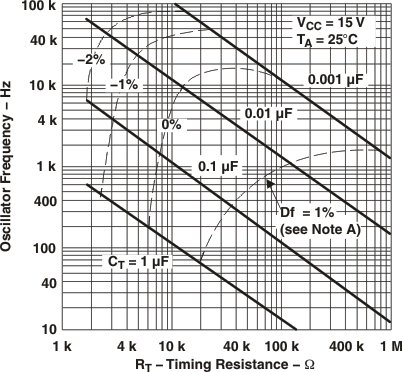
Frequency variation (Δf) is the change in oscillator frequency that occurs over the full temperature range.
Figure 1. Oscillator Frequency and Frequency Variationvs Timing Resistance

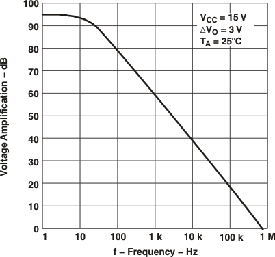
vs Frequency