SLVS220G July 1999 – August 2016 TL7700
PRODUCTION DATA.
- 1 Features
- 2 Applications
- 3 Description
- 4 Revision History
- 5 Pin Configuration and Functions
- 6 Specifications
- 7 Parameter Measurement Information
- 8 Detailed Description
- 9 Application and Implementation
- 10Power Supply Recommendations
- 11Layout
- 12Device and Documentation Support
- 13Mechanical, Packaging, and Orderable Information
Package Options
Mechanical Data (Package|Pins)
Thermal pad, mechanical data (Package|Pins)
- PS|8
Orderable Information
8 Detailed Description
8.1 Overview
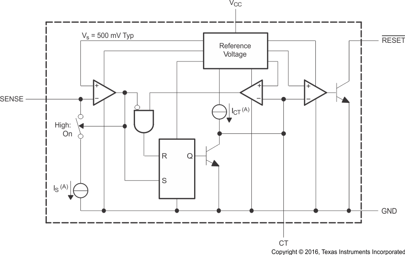
The TL7700 is a bipolar integrated circuit designed for use as a reset controller in microcomputer and microprocessor systems. The SENSE voltage can be set to any value greater than 0.5 V using two external resistors. The hysteresis value of the sense voltage also can be set by the same resistors. The device includes a precision voltage reference, fast comparator, timing generator, and output driver, so it can generate a power-on reset signal in a digital system.
The TL7700 has an internal 1.5-V temperature-compensated voltage reference from which all function blocks are supplied. Circuit function is very stable, with supply voltage in the 1.8-V to 40-V range. Minimum supply current allows use with ac line operation, portable battery operation, and automotive applications.
8.2 Functional Block Diagram

8.3 Feature Description
8.3.1 Sense-Voltage Setting
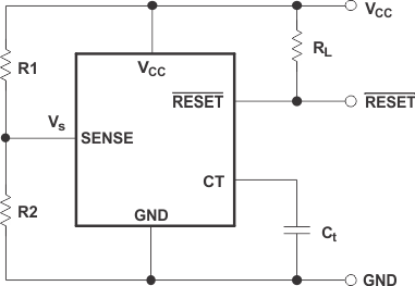
The SENSE terminal input voltage, Vs, of the TL7700 typically is 500 mV. By using two external resistors, the circuit designer can obtain any sense voltage over 500 mV. In Figure 18, the sensing voltage, Vs', is calculated as:
where
- Vs = 500 mV typ at TA = 25°C
At room temperature, Vs has a variation of 500 mV ± 5 mV. In the basic circuit shown in Figure 18, variations of [±5 ± (R1 + R2)/R2] mV are superimposed on Vs.
 Figure 18. Setting the Sense Voltage
8.3.2 Sense-Voltage Hysteresis Setting
If the sense voltage (Vs') does not have hysteresis in it, and the voltage on the sensing line contains ripples, the resetting of TL7700 is unstable. Hysteresis is added to the sense voltage to prevent such problems. As shown in Figure 19, the hysteresis (Vhys) is added, and the value is determined as:
where
- Is = 2.5 μA typ at TA = 25°C
At room temperature, Is has variations of 2.5 µA ± 0.5 µA. Therefore, in the circuit shown in Figure 18, Vhys has variations of (±0.5 × R1) µV. In circuit design, it is necessary to consider the voltage-dividing resistor tolerance and temperature coefficient in addition to variations in Vs and Vhys.

8.3.3 Output Pulse-Duration Setting
Constant-current charging starts on the timing capacitor when the sensing-line voltage reaches the TL7700 sense voltage. When the capacitor voltage exceeds the threshold level of the output drive comparator, RESET changes from a low to a high level. The output pulse duration is the time between the point when the sense-pin voltage exceeds the threshold level and the point when the RESET output changes from a low level to a high level. When the TL7700 is used for system power-on reset, the output pulse duration, tpo, must be set longer than the power rise time. The value of tpo is:
where
- Ct is the timing capacitor in farads
There is a limit on the device response speed. Even if Ct = 0, tpo is not 0, but approximately 5 µs to 10 µs. Therefore, when the TL7700 is used as a comparator with hysteresis without connecting Ct, switching speeds (tr/tf, tpo/tpd, and so forth) must be considered.
8.4 Device Functional Modes
Figure 20 describes how the RESET output pin responds to a change in the voltage at the sense pin. When the sense pin drops below 500 mV, the RESET pin is pulled low.
