DATA SHEET
TLC5954 48-Channel, Constant-Current LED Driver with Global Brightness Control, LED Open-Short Detection, and Power-Save Mode
1 Features
- 48 Constant-Current Sink Output Channels with On or Off Control
- Current Capability:
- 34.9 mA for 32 Channels
- 24.4 mA 16 Channels
- No External Resistor for Current Setting
- Maximum Current Control (MC): 3 Bits (8 Steps)
- Global Brightness Control (BC) for Each Color Group: 7 Bits (128 Steps), Three Groups
- LED Power-Supply Voltage: Up to 10 V
- VCC = 3.0 V to 3.6 V
- Constant-Current Accuracy:
- Channel-to-Channel = ±1% (typ), ±3% (max)
- Device-to-Device = ±2% (typ), ±4% (max)
- Data Transfer Rate: 30 MHz
- BLANK Pulse Duration: 40 ns (min)
- LED Open Detection (LOD)
- LED Short Detection (LSD)
- Power-Save Mode (PSM): 7-µA Consumption, High-Speed Recovery
- Undervoltage Lockout Sets Default Data
- Delayed Switching Minimizes Inrush Current
- Operating Temperature: –40°C to +85°C
2 Applications
- LED Video Displays
- Variable Message Signs (VMS)
- Illumination
3 Description
The TLC5954 is a 48-channel, constant-current sink LED driver. Each channel can be turned on or off by writing data to an internal register. The output channels (OUTXn) are grouped into three groups of 16 channels. Each channel group (R, G, and B) has a 128-step global brightness control (BC) function. The maximum current value of all 48 channels can be set with an 8-step maximum current control (MC) function. The device has two error flags: LED open detection (LOD) and LED short detection (LSD). The error flags can be read via a serial interface port. The device also has a power-save mode that sets the total current consumption to 7 µA (typ) when all outputs are off.
Device Information(1)
| DEVICE NAME | PACKAGE | BODY SIZE |
|---|---|---|
| TLC5954 | VQFN (56) | 8 mm × 8 mm |
- For all available packages, see the orderable addendum at the end of the datasheet.
Application Circuit

4 Revision History
| Date | Revision | Notes |
|---|---|---|
| April 2014 | * | Initial release. |
5 Pin Configuration and Functions
RTQ Package
VQFN-56
(Top View)
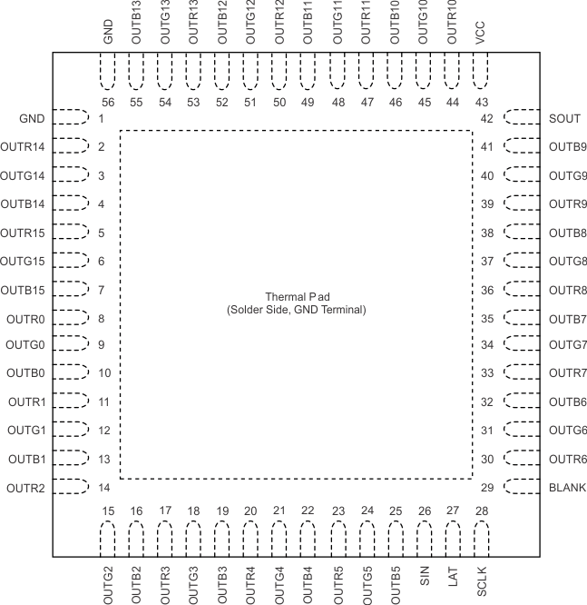
Pin Functions
| PIN | I/O | DESCRIPTION | |
|---|---|---|---|
| NAME | NO. | ||
| GND | 1, 56 | — | Ground. All GND pins are connected internally. |
| OUTR0 to OUTR15 | 2, 5, 8, 11, 14, 17, 20, 23, 30, 33, 36, 39, 44, 47, 50, 53 | O | Red LED constant-current outputs (OUTRn). Multiple outputs can be tied together to increase the constant-current capability. Different voltages can be applied to each output. These outputs are turned on or off by the BLANK signal and the data in the output on or off control data latch. |
| OUTG0 to OUTG15 | 3, 6, 9, 12, 15, 18, 21, 24, 31, 34, 37, 40, 45, 48, 51, 54 | O | Green LED constant-current outputs (OUTGn). Multiple outputs can be tied together to increase the constant-current capability. Different voltages can be applied to each output. These outputs are turned on or off by the BLANK signal and the data in the output on or off control data latch. |
| OUTB0 to OUTB15 | 4, 7, 10, 13, 16, 19, 22, 25, 32, 35, 38, 41, 46, 49, 52, 55 | O | Blue LED constant-current outputs (OUTBn). Multiple outputs can be tied together to increase the constant-current capability. Different voltages can be applied to each output. These outputs are turned on or off by the BLANK signal and the data in the output on or off control data latch. |
| SIN | 26 | I | Serial data input of the 49-bit common shift register, Schmitt buffer input. When SIN is high, the LSB is set to 1 for only one SCLK input rising edge. If two SCLK rising edges are input while SIN is high, then the 49-bit shift register LSB and LSB+1 are set to 1. When SIN is low, the LSB is set to 0 at the SCLK input rising edge. |
| LAT | 27 | I | Edge-triggered latch, Schmitt buffer input. The LAT rising edge latches data from the common shift register either into the output on or off data latch or the maximum current control (MC), brightness control (BC), or function control (FC) data latch. When the common shift register data are latched into the on or off data latch, data in the common shift register are simultaneously replaced with SID, which is selected by SIDLD. Refer to the Output On or Off Data Latch and Status Information Data (SID) sections for more details. |
| SCLK | 28 | I | Serial data shift clock, Schmitt buffer input. Data present on SIN are shifted to the 49-bit common shift register LSB with the SCLK rising edge. Data in the shift register are shifted towards the MSB at each SCLK rising edge. The common shift register MSB appears on SOUT. |
| BLANK | 29 | I | Blank all outputs, Schmitt buffer input. When BLANK is high, all constant-current outputs (OUTXn) are forced off. When BLANK is low, all OUTXn are controlled by the on or off control data in the data latch. |
| SOUT | 42 | O | Serial data output of the 49-bit common shift register. SOUT is connected to the MSB of the register. Data are clocked out at the SCLK rising edge. |
| VCC | 43 | — | Power-supply voltage |
| Thermal pad | — | Ground. The thermal pad must be connected to GND on the printed circuit board (PCB). | |
6 Specifications
6.1 Absolute Maximum Ratings
over operating free-air temperature range (unless otherwise noted)(1)| MIN | MAX | UNIT | |||
|---|---|---|---|---|---|
| VCC | Supply voltage(2) | –0.3 | 4.0 | V | |
| VIN | Input voltage range | SIN, SCLK, LAT, BLANK | –0.3 | VCC + 0.3 | V |
| VOUT | Output voltage range | SOUT | –0.3 | VCC + 0.3 | V |
| OUTR0 to OUTR15, OUTG0 to OUTG15, OUTB0 to OUTB15 |
–0.3 | 11 | V | ||
| TJ (max) | Operating junction temperature | 150 | °C | ||
(1) Stresses beyond those listed under Absolute Maximum Ratings may cause permanent damage to the device. These are stress ratings only, and functional operation of the device at these or any other conditions beyond those indicated under Recommended Operating Conditions is not implied. Exposure to absolute-maximum-rated conditions for extended periods my affect device reliability.
(2) All voltages are with respect to device ground pin.
6.2 Handling Ratings
| MIN | MAX | UNIT | |||
|---|---|---|---|---|---|
| Tstg | Storage temperature range | –55 | 150 | °C | |
| V(ESD) | Electrostatic discharge | Human body model (HBM), per ANSI/ESDA/JEDEC JS-001, all pins(1) | –200 | 2000 | V |
| Charged device model (CDM), per JEDEC specification JESD22-C101, all pins(2) | –500 | 500 | V | ||
(1) JEDEC document JEP155 states that 500-V HBM allows safe manufacturing with a standard ESD control process.
(2) JEDEC document JEP157 states that 250-V CDM allows safe manufacturing with a standard ESD control process.
6.3 Recommended Operating Conditions
At TA= –40°C to +85°C, unless otherwise noted.| PARAMETER | TEST CONDITIONS | MIN | NOM | MAX | UNIT | |
|---|---|---|---|---|---|---|
| DC CHARACTERISTICS (VCC = 3 V to 3.6 V) | ||||||
| VCC | Supply voltage | 3.0 | 3.6 | V | ||
| VO | Voltage applied to output | OUTR0 to OUTR15, OUTG0 to OUTG15, OUTB0 to OUTB15 | 10 | V | ||
| VIH | High-level input voltage | SIN, SCLK, LAT, BLANK | 0.7 × VCC | VCC | V | |
| VIL | Low-level input voltage | SIN, SCLK, LAT, BLANK | GND | 0.3 × VCC | V | |
| IOH | High-level output current | SOUT | –2 | mA | ||
| IOL | Low-level output current | SOUT | 2 | mA | ||
| TA | Operating free-air temperature range | –40 | +85 | °C | ||
| TJ | Operating junction temperature range | –40 | +125 | °C | ||
| AC CHARACTERISTICS (VCC = 3 V to 3.6 V) | ||||||
| fCLK (SCLK) | Data shift clock frequency | SCLK | 30 | MHz | ||
| tWH0 | Pulse duration | SCLK | 10 | ns | ||
| tWL0 | SCLK | 10 | ns | |||
| tWH1 | LAT | 15 | ns | |||
| tWH2 | BLANK | 60 | ns | |||
| tWL2 | BLANK | 40 | ns | |||
| tSU0 | Setup time | SIN to SCLK↑ | 4 | ns | ||
| tSU1 | LAT↓ to SCLK↑ | 20 | ns | |||
| tSU2 | SCLK↑ resumes normal mode, BLANK↓, PSMODE bit = 01b | 12 | µs | |||
| tSU3 | LAT↑ for all data latching except all 0s resumes normal mode, BLANK↓, PSMODE bit = 10b | 12 | µs | |||
| tH0 | Hold time | SCLK↑ to SIN | 3 | ns | ||
| tH1 | SCLK↑ to LAT↑ | 10 | ns | |||
6.4 Thermal Information
| THERMAL METRIC(1) | TLC5954 | UNIT | |
|---|---|---|---|
| RTQ (VQFN) | |||
| 56 PINS | |||
| RθJA | Junction-to-ambient thermal resistance | 29.1 | °C/W |
| RθJCtop | Junction-to-case (top) thermal resistance | 16.3 | |
| RθJB | Junction-to-board thermal resistance | 7.7 | |
| ψJT | Junction-to-top characterization parameter | 0.3 | |
| ψJB | Junction-to-board characterization parameter | 7.7 | |
| RθJCbot | Junction-to-case (bottom) thermal resistance | 2.8 | |
(1) For more information about traditional and new thermal metrics, see the IC Package Thermal Metrics application report, SPRA953.
6.5 Electrical Characteristics
At TA = –40°C to +85°C and VCC = 3.0 V to 3.6 V, unless otherwise noted. Typical values are at TA = +25°C and VCC = 3.3 V.| PARAMETER | TEST CONDITIONS | MIN | TYP | MAX | UNIT | ||
|---|---|---|---|---|---|---|---|
| VOH | High-level output voltage | IOH = –2 mA at SOUT | VCC – 0.4 | VCC | V | ||
| VOL | Low-level output voltage | IOL = 2 mA at SOUT | 0.4 | V | |||
| VLOD0 | LED open-detection threshold | LODVLT = 000b | 0.15 | 0.20 | 0.25 | V | |
| VLOD1 | LODVLT = 001b, 101b, 110b, 111b | 0.25 | 0.30 | 0.35 | V | ||
| VLOD2 | LODVLT = 010b | 0.35 | 0.40 | 0.45 | V | ||
| VLOD3 | LODVLT = 011b | 0.45 | 0.50 | 0.55 | V | ||
| VLOD4 | LODVLT = 100b | 0.55 | 0.60 | 0.65 | V | ||
| VLSD0 | LED short-detection threshold | LSDVLT = 00b | 0.45 × VCC | 0.50 × VCC | 0.55 × VCC | V | |
| VLSD1 | LSDVLT = 01b | 0.65 × VCC | 0.70 × VCC | 0.75 × VCC | V | ||
| VLSD2 | LSDVLT = 10b, 11b | 0.85 × VCC | 0.90 × VCC | 0.95 × VCC | V | ||
| IIN | Input current | VIN = VCC or GND at SIN, SCLK, LAT, and BLANK | –1 | 1 | μA | ||
| ICC0 | Supply current (VCC) | SIN, SCLK, LAT = GND, BLANK = VCC, VOUTXn = 1 V, BCX = 7Fh, MC = 0h (IOUTRn, IOUTGn = 2.9-mA target, IOUTBn = 2.0-mA target)(5) | 15 | 19 | mA | ||
| ICC1 | SIN, SCLK, LAT = GND, BLANK = VCC, VOUTXn = 1 V, BCX = 7Fh, MC = 5h (IOUTRn, IOUTGn = 17.4-mA target, IOUTBn = 12.2-mA target) | 17.5 | 22 | mA | |||
| ICC2 | SIN, SCLK, LAT, BLANK = GND, all OUTXn = on, VOUTXn = 1 V, BCX = 7Fh, MC = 5h | 17.5 | 22 | mA | |||
| ICC3 | SIN, SCLK, LAT, BLANK = GND, all OUTXn = on, VOUTXn = 1 V, BCX = 7Fh, MC = 7h (IOUTRn, IOUTGn = 34.9-mA target, IOUTBn = 24.4-mA target) | 20.5 | 25.5 | mA | |||
| ICC4 | In power-save mode, SIN, SCLK, LAT = GND, BLANK = VCC |
7 | 60 | µA | |||
| IOLC0 | Constant output current | All OUTXn = on, VOUTXn = VOUTfix = 1 V, BC = 7Fh, MC = 7h, at OUTR0 to OUTR15 and OUTG0 to OUTG15 |
32.5 | 34.9 | 37.3 | mA | |
| IOLC1 | All OUTXn = on, VOUTXn = VOUTfix = 1 V, BC = 7Fh, MC = 7h, at OUTB0 to OUTB15 |
22.7 | 24.4 | 26.1 | mA | ||
| IOLKG | Output leakage current | BLANK = VCC, VOUTXn = VOUTfix = 10 V, MC = 7h, at OUTXn | TJ = +25°C | 0.1 | µA | ||
| TJ = +85°C | 0.2 | µA | |||||
| TJ = +125°C | 0.5 | µA | |||||
| ΔIOLC0 | Constant-current error (channel-to-channel)(1) |
All OUTXn = on, BCX = 7Fh, VOUTXn = VOUTfix = 1 V, MC = 7h, at same color group (OUTXn) | ±1% | ±3% | |||
| ΔIOLC1 | Constant-current error (device-to-device)(2) |
All OUTXn = on, BCX = 7Fh, VOUTXn = VOUTfix = 1 V, MC = 7h, at same color group (OUTXn) | ±0.5% | ±3% | |||
| ΔIOLC2 | Line regulation(3) | All OUTXn = on, BCX = 7Fh, VOUTXn = VOUTfix = 1 V, MC = 7h, at OUTXn | ±0.5 | ±1 | %/V | ||
| ΔIOLC3 | Load regulation(4) | All OUTXn = on, BCX = 7Fh, VOUTXn = 1 V to 3 V, VOUTfix = 1 V, MC = 7h, at OUTXn | ±1 | ±3 | %/V | ||
(1) The deviation of each output in the same color group (OUTRn, OUTGn, OUTBn) from the average of the same OUTXn group constant-current. Deviation is calculated by the formula:

, where X = R, G, or B, and n = 0 to 15.
, where X = R, G, or B, and n = 0 to 15.
(2) The deviation of the OUTXn constant-current average from the ideal constant-current value. Deviation is calculated by the formula:

Ideal current is 34.9 mA for OUTRn and OUTGn. Ideal current is 24.4 mA for OUTBn with MC data equal to 7h.
, where X = R, G, or B, and n = 0 to 15.
Ideal current is 34.9 mA for OUTRn and OUTGn. Ideal current is 24.4 mA for OUTBn with MC data equal to 7h.
, where X = R, G, or B, and n = 0 to 15.
(3) Line regulation is calculated by the formula:

X = R, G, or B. n = 0 to 15.
X = R, G, or B. n = 0 to 15.
(4) Load regulation is calculated by the equation:

, where X = R, G, or B, and n = 0 to 15.
, where X = R, G, or B, and n = 0 to 15.
(5) X = R, G, and B. n = 0 to 15.
6.6 Switching Characteristics
At TA = –40°C to +85°C, VCC = 3.0 V to 3.6 V, CL = 15 pF, RL = 100 Ω for OUTRn and OUTGn, RL = 150 Ω for OUTBn,MC = 7h, and VLED = 4.5 V, unless otherwise noted. Typical values at TA = +25°C and VCC = 3.3 V.
| PARAMETER | TEST CONDITIONS | MIN | TYP | MAX | UNIT | |
|---|---|---|---|---|---|---|
| tR0 | Rise time | SOUT | 2 | 5 | ns | |
| tR1 | OUTXn, BCX = 7Fh(3) | 20 | 50 | ns | ||
| tF0 | Fall time | SOUT | 2 | 5 | ns | |
| tF1 | OUTXn, BCX = 7Fh | 20 | 50 | ns | ||
| tD0 | Propagation delay(1) | SCLK↑ to SOUT | 13 | 23 | ns | |
| tD1 | LAT↑ to OUTR0 on to off or OUTR0 off to on, BCX = 7Fh | 30 | 60 | ns | ||
| tD2 | BLANK↓↑ to OUTR0 on to off or OUTR0 off to on, BCX = 7Fh | 30 | 60 | ns | ||
| tD3 | OUTRn on to OUTGn on, OUTGn on to OUTBn on, and OUTBn on to the next OUTRn on, BCX = 7Fh | 1.5 | 5 | ns | ||
| tD4 | OUTRn off to OUTGn off, OUTGn off to OUTBn off, and OUTBn off to the next OUTRn off, BCX = 7Fh | 1.5 | 5 | ns | ||
| tD5 | LAT↑ to power-save mode by writing data for all OUTXn off | 150 | 300 | ns | ||
| tON_ERR | Output on-time error(2) | OUTXn on or off data = all 1s, BCX = 7Fh, 40-ns BLANK low-level one-shot pulse input | –35 | 35 | ns | |
(1) tD3 (OUTRn on to OUTGn on, OUTGn on to OUTBn on, and OUTBn on to the next OUTRn on) and tD4 (OUTRn off to OUTGn off, OUTGn off to OUTBn off, and OUTBn off to the next OUTRn off) are calculated by:
tD3 (ns) = (the propagation delay between OUTR0 on to OUTB7 on) / 47 and
tD4 (ns) = (the propagation delay between OUTR0 off to OUTB7 off) / 47.
tD3 (ns) = (the propagation delay between OUTR0 on to OUTB7 on) / 47 and
tD4 (ns) = (the propagation delay between OUTR0 off to OUTB7 off) / 47.
(2) Output on-time error (tON_ERR) is calculated by the formula: tON_ERR (ns) = tOUT_ON – BLANK low-level pulse duration.
tOUT_ON is the actual on-time of OUTXn.
tOUT_ON is the actual on-time of OUTXn.
(3) X = R, G, or B. n = 0 to 15.
6.7 Typical Characteristics
At TA = +25°C and VCC = 3.3 V, unless otherwise noted.
| BCR, BCG = 7Fh |
(OUTRn, OUTGn)

| BCR = BCG = 7Fh | MC = 7 |
(OUTRn, OUTGn)

| BCR = 7Fh | MC = 7 |

| BCB = 7Fh | MC = 7 |

| BCG = 7Fh | MC = 7h |

| BCR = BCG = 7Fh |
(OUTRn, OUTGn)

| SIN = 15 MHz | SCLK = 30 MHz | BCX = 7Fh |
| MC = 0h to 7h | All OUTXn = On | BLANK = Low |
| SOUT = No Load | VOUT = 0.8 V | |

| VCC = 3.3 V | MC = 7h | BCX = 7Fh | VLED = 4.5 V | ||
| RL = 100 Ω (OUTRn, OUTGn) | RL = 150 Ω (OUTBn) | ||||
| CL = 15 pF | BLANK Low Pulse Duration = 40 ns | ||||

| BCB = 7Fh |
(OUTBn)

| BCB = 7Fh | MC = 7 |
(OUTBn)

| BCG = 7Fh | MC = 7 |

| BCR = 7Fh | MC = 7h |

| BCB = 7Fh | MC = 7 |

| BCB = 7Fh |
(OUTBn)

| SIN = 15 MHz | BCX = 7Fh | MC = 5h |
| All OUTXn = On | SCLK = 30 MHz | BLANK = Low |
| SOUT = No Load | VOUT = 0.8 V | |
| TA = –40°C to +85°C | ||
