SBVS225B March 2013 – May 2014 TLC5973
PRODUCTION DATA.
- 1 Features
- 2 Applications
- 3 Description
- 4 Revision History
- 5 Pin Configuration and Functions
- 6 Specifications
- 7 Parameter Measurement Information
- 8 Detailed Description
- 9 Applications and Implementation
- 10Power Supply Recommendations
- 11Layout
- 12Device and Documentation Support
- 13Mechanical, Packaging, and Orderable Information
Package Options
Mechanical Data (Package|Pins)
- D|8
Thermal pad, mechanical data (Package|Pins)
Orderable Information
8 Detailed Description
8.1 Overview
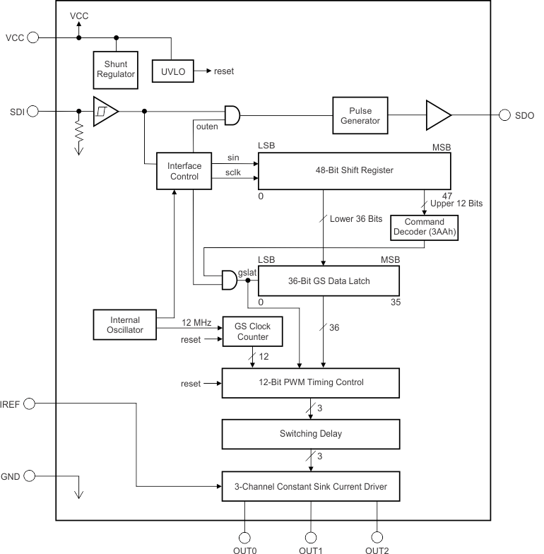
The TLC5973 is 3-channel, 50-mA, constant-current LED driver that can control LED on-time with pulse width modulation (PWM) in 4096 steps for grayscale (GS) control. A maximum of 68 billion colors can be generated with red, green, and blue LEDs connected to each constant-current output. Furthermore, a reference clock generator is implemented in the device, which means that the reference clock for PWM timing control is not required to be supplied from an external clock generator or controller.
The device adopts a single-wire input or output system. Therefore, communication wire cost and communication wire failure are reduced. Further wire cost reduction can be attained when supplying power to the device. One wire can be eliminated because the device power can be generated from the LED power line with the internal shunt regulator.
The device can reduce the amount of incorrect data writes because the one-write command is required to write GS data to the device. The maximum data transfer rate for the device is 3 Mbps. Therefore, GS data can be updated with a high refresh rate even if many devices are connected in series. The number of TLC5973 devices connected in series is not limited because the TLC5973 has an internal buffer that drives the output signal.
8.3 Feature Description
8.3.1 Grayscale (GS) Control
This control feature is a 12-bit (4096-step) grayscale (GS) control that provides a wide range of color generation. 68 billion colors can be generated with the red, green, and blue LEDs. Connect the LEDs to the device OUTn pins, as described in the Applications and Implementation section.
8.3.2 EasySet and Shunt Regulator
This device includes a single-wire serial interface (EasySet) and a shunt regulator. The total number of wires for power supply and data write operations can be reduced with the EasySet and shunt regulator included in the design.
8.3.3 No Limit Cascading
This feature results in no limitation on the number of total cascaded devices used in series in an application. This advantage is attained because a timing-adjusted pulse generator is implemented in the device.
8.3.4 Constant Sink Current Value
The output current value of each channel (IOLC) is programmed by a single resistor (RIREF) that is placed between the IREF and GND pins. The current value can be calculated by Equation 1:

where
- VIREF = the internal reference voltage on IREF (typically 1.20 V), and
- IOLC = 2 mA to 50 mA
IOLC is the current for each output. Each output sinks IOLC current when it is turned on. RIREF must be between
1 kΩ and 27 kΩ in order to hold IOLC between 50 mA (typ) and 1.93 mA (typ). Otherwise, the output may be unstable. Refer to Figure 1 and Table 1 for the constant-current sink values for specific external resistor values.
Table 1. Constant-Current Output versus
External Resistor Value
| IOLC (mA) | RIREF (kΩ, typ) |
|---|---|
| 50 | 1.04 |
| 45 | 1.16 |
| 40 | 1.30 |
| 35 | 1.49 |
| 30 | 1.74 |
| 25 | 2.08 |
| 20 | 2.60 |
| 15 | 3.47 |
| 10 | 5.21 |
| 5 | 10.4 |
| 2 | 26.0 |
8.3.5 Connector Design
When the connector pin of the device application printed circuit board (PCB) is connected or disconnected to other PCBs, the power must be turned off to avoid device malfunction or failure. Furthermore, designing the connector GND pin to be longer than other pins (as shown in Figure 12) is preferable. This arrangement allows the GND line to either be connected first or disconnected last, which is imperative for proper device function.
 Figure 12. Connector Pin Design Application
8.4 Device Functional Modes
8.4.1 Grayscale (GS) Function (PWM Control)
The TLC5973 can adjust the brightness of each output channel using a pulse width modulation (PWM) control scheme. The PWM data bit length for each output is 12 bits. The architecture of 12 bits per channel results in 4096 brightness steps, from 0% to 99.98% on-time duty cycle.
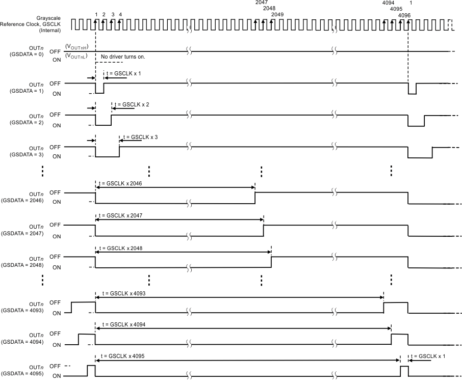
The PWM operation for OUTn is controlled by an 12-bit grayscale (GS) counter. The GS counter increments on each internal GS clock (GSCLK) rising edge. All OUTn are turned on when the GS counter is ‘1’, except when OUTn are programed to GS data '0' in the 36-bit GS data latch. After turning on, each output is turns off when the GS counter value exceeds the programmed GS data for the output. The GS counter resets to 000h and all outputs are forced off when the GS data are written to the 36-bit GS data latch. Afterwards, the GS counter begins incrementing and PWM control is started from the next internal GS clock.
Table 2 summarizes the GS data values versus the output ideal on-time duty cycle. Furthermore, actual on-time differs from the ideal on-time because the output drivers and control circuit have some timing delay. When the device is powered on, all outputs are forced off and remain off until the non-zero GS data are written to the 36-bit GS data latch.
Table 2. Output Duty Cycle and Total On-Time versus GS Data
| GS DATA | NO. OF GSCLKs OUTn TURNS ON | NO. OF GSCLKs OUTn TURNS OFF | TOTAL IDEAL TIME (µs) | ON-TIME DUTY (%) | |
|---|---|---|---|---|---|
| DECIMAL | HEX | ||||
| 0 | 0 | Off | Off | 0 | 0 |
| 1 | 1 | 1 | 2 | 0.08 | 0.02 |
| 2 | 2 | 1 | 3 | 0.17 | 0.05 |
| — | — | — | — | — | — |
| 255 | 0FE | 1 | 256 | 21.25 | 6.23 |
| 256 | 0FF | 1 | 257 | 21.33 | 6.25 |
| 257 | 100 | 1 | 258 | 21.42 | 6.27 |
| — | — | — | — | — | — |
| 511 | 1FF | 1 | 512 | 42.58 | 12.48 |
| 512 | 200 | 1 | 513 | 42.67 | 12.50 |
| 513 | 201 | 1 | 514 | 42.75 | 12.52 |
| — | — | — | — | — | — |
| 1023 | 3FF | 1 | 1024 | 85.25 | 24.98 |
| 1024 | 400 | 1 | 1025 | 85.33 | 25.00 |
| 1025 | 401 | 1 | 1026 | 85.42 | 25.00 |
| — | — | — | — | — | — |
| 2047 | 7FF | 1 | 2048 | 170.6 | 49.98 |
| 2048 | 800 | 1 | 2049 | 170.7 | 50.00 |
| 2049 | 801 | 1 | 2050 | 170.8 | 50.02 |
| — | — | — | — | — | — |
| 4093 | FFD | 1 | 4094 | 341.1 | 99.93 |
| 4094 | FFE | 1 | 4095 | 341.2 | 99.95 |
| 4095 | FFF | 1 | 4096 | 341.3 | 99.98 |
8.4.1.1 PWM Control
The GS counter keeps track of the number of grayscale reference clocks (GSCLKs) from the internal oscillator. Each output stays on while the counter is less than or equal to the programmed GS value. Each output turns off when the GS counter is greater than the GS value in the 36-bit GS data latch. Figure 13 illustrates the PWM operation timing.
8.4.2 One-Wire Interface (EasySet) Data Writing Method
There are four sequences to write GS data into the TLC5973 via a single-wire interface. This section discusses each sequence in detail.
8.4.2.1 Data Transfer Rate (tCYCLE) Measurement Sequence
The TLC5973 measures the time between the first and second SDI rising edges either after the device is powered up or when the GS data latch sequence is executed (as described in the GS Data Latch Sequence (GSLAT) section) and the time is internally stored as tCYCLE. tCYCLE serves as a base time used to recognize one complete data write operation, a 48-bit data write operation, and a GS data write operation to the GS data latch. tCYCLE can be set between 0.33 µs and 10 µs (fCLK(SDI) = 100 kHz to 3000 kHz). In this sequence, two instances of data ‘0’ are written to the LSB side of the 48-bit shift register. Figure 14 shows the tCYCLE measurement timing.
 Figure 14. Data Transfer Rate (tCYCLE) Measurement
8.4.2.2 Data ‘0’ and Data ‘1’ Write Sequence (Data Write Sequence)
When the second SDI rising edge is not input before 0.9 × tCYCLE elapses from the first SDI rising edge input, the data are recognized as '0'. When the second SDI rising edge is input before 50% of tCYCLE elapses from the first SDI rising edge input, the data are recognized as '1'. This write sequence must be repeated 46 times after the tCYCLE measurement sequence in order to send the write command to the higher 10-bit (3AAh) and 36-bit GS data. Figure 15 shows the data ‘0’ and ‘1’ write timing.
 Figure 15. Data ‘0’ and ‘1’ Write Operation
8.4.2.3 One Communication Cycle End of Sequence (EOS)
One communication cycle end of sequence (EOS) must be input after the 48-bit data are written because the TLC5973 does not count the number of input data. When SDI is held low for the EOS hold time (tH0), the 48-bit shift register values are locked and a buffered SDI signal is output from SDO to transfer GS data to the next device. Figure 16 shows the EOS timing.
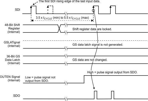 Figure 16. End of Sequence (EOS)
8.4.2.4 GS Data Latch (GSLAT) Sequence
A GS data latch (GSLAT) sequence must be input after the 48-bit data for all cascaded devices are written. When SDI is held low for the data latch hold time (tH1), the 48-bit shift register data in all devices are copied to the GS data latch in each device. Furthermore, PWM control starts with the new GS data at the same time. Figure 17 shows the GSLAT timing.
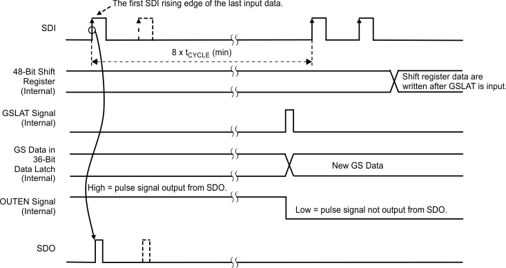 Figure 17. GS Data Latch Sequence (GSLAT)
8.5 Programming
8.5.1 Controlling Devices Connected in Series
The 12-bit write command and 36-bit grayscale (GS) data for OUT0 to OUT2 (for a total of 48 bits of data) must be written to the device. Figure 18 shows the 48-bit data packet configuration. When multiple devices are cascaded (as shown in Figure 19), N times the packet must be written into each TLC5973 in order to control all devices. There is no limit on how many devices can be cascaded, as long as proper VCC voltage is supplied. The packet for all devices must be written again whenever any GS data changes.
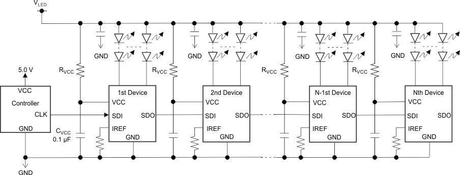 Figure 19. Cascade Connection of N TLC5973 Units (Internal Shunt Regulator Mode)
The function setting write procedure and display control is:
- Power-up VCC (VLED); all OUTn are off because GS data are not written yet.
- Write the 48-bit data packet (MSB-first) for the first device using tCYCLE and the data write sequences illustrated in Figure 14 and Figure 15. The first 12 bits of the 48-bit data packet are used as the write command. The write command must be 3AAh (001110101010b); otherwise, the 36-bit GS data in the 48-bit shift register are not copied to the 36-bit GS data latch.
- Execute one communication cycle EOS (refer to Figure 16) for the first device.
- Write the 48-bit data packet for the second TLC5973 as described step 2. However, tCYCLE should be set to the same timing as the first device.
- Execute one communication cycle EOS for the second device.
- Repeat steps 4 and 5 until all devices have GS data.
- The number of total bits is 48 × N. After all data are written, execute a GSLAT sequence as described in Figure 17 in order to copy the 36-bit LSBs in the 48-bit shift resister to the 36-bit GS data latch in each device; PWM control starts with the written GS data at the same time.
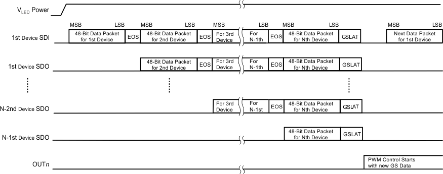 Figure 20. Data Packet Input Order for N TLC5973 Units
8.6 Register Maps
8.6.1 Register and Data Latch Configuration
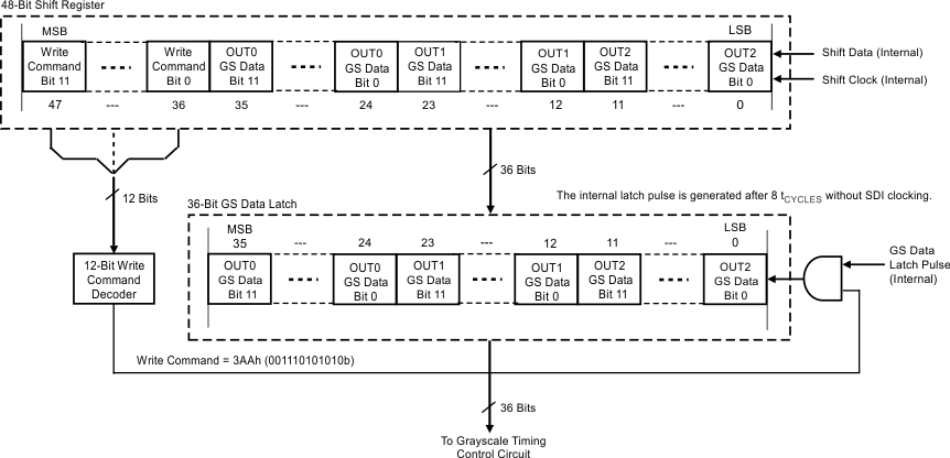
The TLC5973 has a 48-bit shift register and a 36-bit data latch that stores GS data. When the internal GS data latch pulse is generated and the data of the 12 MSBs in the shift register are 3AAh, the lower 36-bit data in the 48-bit shift register are copied into the 36-bit GS data latch. If the data of the 12 MSBs is not 3AAh, the 36-bit data are not copied into the 36-bit GS data latch. Figure 21 shows the shift register and GS data latch configurations. Table 3 shows the 48-bit shift register bit assignment.
Table 3. 48-Bit Shift Register Data Bit Assignment
| BITS | BIT NAME | CONTROLLED CHANNEL/FUNCTIONS |
|---|---|---|
| 0 to 11 | GSOUT2 | GS data bits 0 to 11 for OUT2 |
| 12 to 23 | GSOUT1 | GS data bits 0 to 11 for OUT1 |
| 24 to 35 | GSOUT0 | GS data bits 0 to 11 for OUT0 |
| 36 to 47 | WRTCMD | Data write command (3AAh) for GS data. The lower 36-bit GS data in the 48-bit shift register are copied to the GS data latch when the internal GS latch is generated (when these data bits are 3AAh, 001110101010b). |
