SLVSEB5A July 2018 – August 2018 TLC6C5716-Q1
PRODUCTION DATA.
- 1 Features
- 2 Applications
- 3 Description
- 4 Revision History
- 5 Pin Configuration and Functions
- 6 Specifications
-
7 Detailed Description
- 7.1 Overview
- 7.2 Functional Block Diagram
- 7.3
Feature Description
- 7.3.1 Maximum Constant-Sink-Current Setting
- 7.3.2 Brightness Control and Dot Correction
- 7.3.3 Grayscale Configuration
- 7.3.4
Diagnostics
- 7.3.4.1 LED Diagnostics
- 7.3.4.2 Adjacent-Pin-Short Check
- 7.3.4.3 IREF-Short and IREF-Open Detection
- 7.3.4.4 Pre-Thermal Warning Flag
- 7.3.4.5 Thermal Error Flag
- 7.3.4.6 Negate-Bit Toggle
- 7.3.4.7 LOD_LSD Self-Test
- 7.3.4.8 ERR Pin
- 7.3.4.9 ERROR Clear
- 7.3.4.10 Global Reset
- 7.3.4.11 Slew Rate Control
- 7.3.4.12 Channel Group Delay
- 7.4 Device Functional Modes
- 7.5 Programming
- 7.6 Register Maps
- 8 Application and Implementation
- 9 Power Supply Recommendations
- 10Layout
- 11Device and Documentation Support
- 12Mechanical, Packaging, and Orderable Information
Package Options
Mechanical Data (Package|Pins)
- DAP|38
Thermal pad, mechanical data (Package|Pins)
7.3.3 Grayscale Configuration
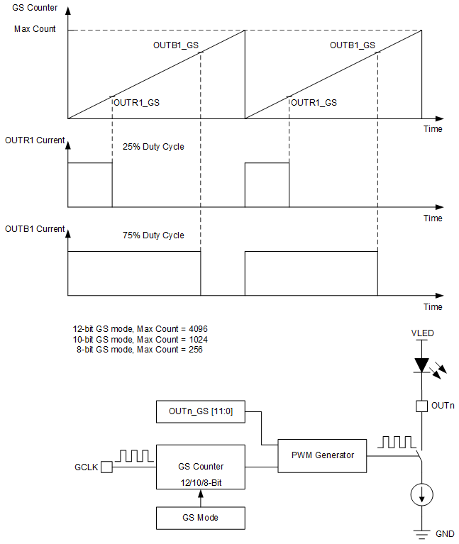
The TLC6C5716-Q1 device implements a grayscale configuration function to realize an individual PWM dimming function for the output channels. The grayscale has three global configuration modes, 12-bit, 10-bit and 8-bit. The GCLK input provides the clock source for the internal PWM generator. The GS counter counts the GCLK number and compares the number with channel grayscale register value, and the output channel turns off when the GS counter value reaches the grayscale register value. Figure 22 shows the detailed block diagram of the PWM generator.
To start a new PWM cycle, users can use two methods. One is to toggle the BLANK pin after the GS counter reaches the maximum count value, because BLANK low resets the GS counter and BLANK high restarts the GS counter. Another is to pull BLANK high and set the AUTO_REPEAT&TIMING_RESET register bit to 1, Table 12. The PWM starts a new cycle automatically after the GS counter reaches its maximum count value.
 Figure 22. PWM Generator