SLLSFM6 June 2021 TLIN2022A-Q1
PRODUCTION DATA
- 1 Features
- 2 Applications
- 3 Description
- 4 Description (Continued)
- 5 Revision History
- 6 Pin Configuration and Functions
- 7 Specifications
- 8 Parameter Measurement Information
-
9 Detailed Description
- 9.1 Overview
- 9.2 Functional Block Diagram
- 9.3
Feature Description
- 9.3.1 LIN (Local Interconnect Network) Bus
- 9.3.2 TXD
- 9.3.3 RXD (Receive Output)
- 9.3.4 VSUP (Supply Voltage)
- 9.3.5 GND (Ground)
- 9.3.6 EN (Enable Input)
- 9.3.7 Protection Features
- 9.3.8 TXD Dominant Time Out (DTO)
- 9.3.9 Bus Stuck Dominant System Fault: False Wake-Up Lockout
- 9.3.10 Thermal Shutdown
- 9.3.11 Undervoltage on VSUP
- 9.3.12 Unpowered Device and LIN Bus
- 9.4 Device Functional Modes
- 10Application Information Disclaimer
- 11Layout
- 12Device and Documentation Support
- 13Mechanical, Packaging, and Orderable Information
Package Options
Mechanical Data (Package|Pins)
Thermal pad, mechanical data (Package|Pins)
- DMT|14
Orderable Information
10.2 Typical Application
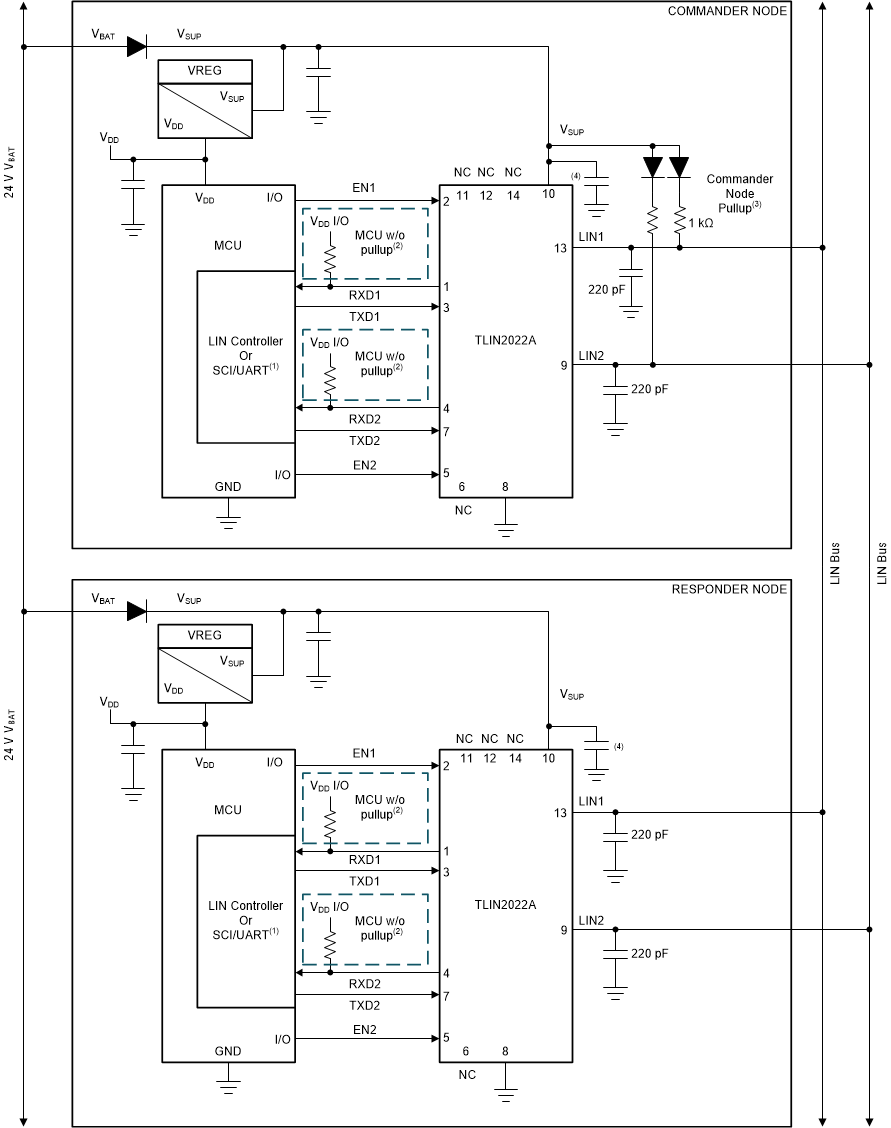
The device comes with an integrated 45 kΩ pull-up resistor and series diode for responder node applications. For commander node applications, an external 1 kΩ pull-up resistor with series blocking diode can be used. Figure 10-1 shows the device being used in both commander mode and responder mode applications.

If RXD on MCU or LIN responder has internal
pullup; no external pullup resistor is needed.
If RXD on MCU or LIN responder does not have an
internal pullup requires external pullup resistor
Commander node applications require and external 1 kΩ
pullup resistor and serial diode.
Decoupling capacitor values are
system dependent but usually have 100 nF, 1 µF and ≥10 µF
Figure 10-1 Typical
LIN Bus