SBOS551D March 2011 – January 2025 TLV3011-Q1 , TLV3011B-Q1 , TLV3012-Q1 , TLV3012B-Q1
PRODUCTION DATA
- 1
- 1 Features
- 2 Applications
- 3 Description
- 4 Pin Configuration and Functions
- 5 Specifications
- 6 Typical Characteristics
- 7 Detailed Description
- 8 Application and Implementation
- 9 Device and Documentation Support
- 10Revision History
- 11Mechanical, Packaging, and Orderable Information
Package Options
Mechanical Data (Package|Pins)
Thermal pad, mechanical data (Package|Pins)
Orderable Information
8.3.1 Power-On Reset
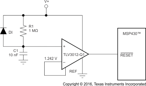
The reset circuit shown below provides a time-delayed release of reset to the MSP430™ microcontroller. Operation of the circuit is based on a stabilization time constant of the supply voltage, rather than on a predetermined voltage value. The negative input is a reference voltage created by the internal voltage reference. The positive input is an RC circuit that provides a power-up delay. When power is applied, the output of the comparator is low, holding the processor in the reset condition. Only after allowing time for the supply voltage to stabilize does the positive input of the comparator become higher than the negative input, resulting in a high output state, releasing the processor for operation. The stabilization time required for the supply voltage is adjustable by the selection of the RC component values. Use of a lower-valued resistor in this portion of the circuit does not increase current consumption, because no current flows through the RC circuit after the supply has stabilized.
 Figure 8-5 TLV3012-Q1 Configured as Power-Up Reset Circuit for the MSP430™ Microcontroller
The reset delay needed depends on the power-up characteristics of the system power supply. R1 and C1 are selected to allow enough time for the power supply to stabilize. D1 provides rapid reset if power is lost. In this example, the R1 × C1 time constant is 10 ms.