SBOS551C march 2011 – april 2023 TLV3011-Q1 , TLV3011B-Q1 , TLV3012-Q1 , TLV3012B-Q1
PRODUCTION DATA
- 1 Features
- 2 Applications
- 3 Description
- 4 Revision History
- 5 Pin Configuration and Functions
-
6 Specifications
- 6.1 Absolute Maximum Ratings TLV3012-Q1 DCK Package Only
- 6.2 Absolute Maximum Ratings - TLV301x-Q1 DBV Package, TLV3011B-Q1 and TLV3012B-Q1
- 6.3 ESD Ratings
- 6.4 Thermal Information - TLV3012-Q1 DCK Package Only
- 6.5 Thermal Information- TLV301x-Q1 DBV Package, TLV3011B-Q1 and TLV3012B-Q1
- 6.6 Recommended Operating Conditions
- 6.7 Electrical Characteristics - TLV3012-Q1 DCK Package Only
- 6.8 Switching Characteristics - TLV3012-Q1 DCK Package Only
- 6.9 Electrical Characteristics- TLV301x-Q1 DBV Package, TLV3011B-Q1 and TLV3012B-Q1
- 6.10 Switching Characteristics- TLV301x-Q1 DBV Package, TLV3011B-Q1 and TLV3012B-Q1
- 7 Typical Characteristics - TLV3012-Q1 DCK Package Only
- 8 Typical Characteristics - TLV301x-Q1 DBV Package, TLV3011B-Q1 and TLV3012B-Q1
- 9 Detailed Description
- 10Application and Implementation
- 11Device and Documentation Support
- 12Mechanical, Packaging, and Orderable Information
Package Options
Mechanical Data (Package|Pins)
Thermal pad, mechanical data (Package|Pins)
Orderable Information
10.2.1 Under-Voltage Detection
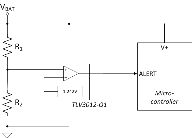
Under-voltage detection is frequently required to alert the system that a battery voltage has dropped below the usable voltage level. Figure 23 shows a simple under-voltage detection circuit using the TLV3012-Q1 which is configured as a non-inverting comparator with the integrated 1.242 V reference is externally connected to the inverting input pin (IN-).
 Figure 10-3 Under-Voltage Detection