SNOSDK2 June   2024 TLV3231-Q1

ADVANCE INFORMATION  

  1.   1
  2. Features
  3. Applications
  4. Description
  5. Pin Configuration and Functions
    1.     Pin Configurations: TLV3231 and TLV3232
  6. Specifications
    1. 5.1 Absolute Maximum Ratings
    2. 5.2 ESD Ratings
    3. 5.3 Recommended Operating Conditions
    4. 5.4 Thermal Information
    5. 5.5 Electrical Characteristics
    6. 5.6 Switching Characteristics
  7. Detailed Description
    1. 6.1 Overview
    2. 6.2 Functional Block Diagrams
    3. 6.3 Feature Description
    4. 6.4 Device Functional Modes
      1. 6.4.1 Inputs
        1. 6.4.1.1 Unused Inputs
      2. 6.4.2 Internal Hysteresis
      3. 6.4.3 Outputs
      4. 6.4.4 ESD Protection
      5. 6.4.5 Power-On Reset (POR)
  8. Application and Implementation
    1. 7.1 Application Information
      1. 7.1.1 Basic Comparator Definitions
        1. 7.1.1.1 Operation
        2. 7.1.1.2 Propagation Delay
        3. 7.1.1.3 Overdrive Voltage
      2. 7.1.2 Hysteresis
        1. 7.1.2.1 Inverting Comparator With Hysteresis
        2. 7.1.2.2 Non-Inverting Comparator With Hysteresis
    2. 7.2 Typical Applications
      1. 7.2.1 Low-Side Current Sensing
        1. 7.2.1.1 Design Requirements
        2. 7.2.1.2 Detailed Design Procedure
    3. 7.3 Power Supply Recommendations
    4. 7.4 Layout
      1. 7.4.1 Layout Guidelines
      2. 7.4.2 Layout Example
  9. Device and Documentation Support
    1. 8.1 Documentation Support
      1. 8.1.1 Related Documentation
    2. 8.2 Receiving Notification of Documentation Updates
    3. 8.3 Support Resources
    4. 8.4 Trademarks
    5. 8.5 Electrostatic Discharge Caution
    6. 8.6 Glossary
  10. Revision History
  11. 10Mechanical, Packaging, and Orderable Information

Package Options

Mechanical Data (Package|Pins)
Thermal pad, mechanical data (Package|Pins)
Orderable Information

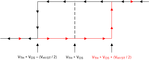
Internal Hysteresis

The device hysteresis transfer curve is shown below. This curve is a function of three components: VTH, VOS, and VHYST:

  • VTH is the actual set voltage or threshold trip voltage.
  • VOS is the internal offset voltage between VIN+ and VIN–. This voltage is added to VTH to form the actual trip point at which the comparator must respond to change output states.
  • VHYST is the internal hysteresis (or trip window) that is designed to reduce comparator sensitivity to noise.

    (1.55mV for the TLV323x-Q1 family)
TLV3231-Q1 TLV3232-Q1 Hysteresis Transfer CurveFigure 6-2 Hysteresis Transfer Curve