SLVS139Z July 1996 – June 2024 TLV431 , TLV431A , TLV431B
PRODUCTION DATA
- 1
- 1 Features
- 2 Applications
- 3 Description
- 4 Pin Configuration and Functions
- 5 Specifications
- 6 Parameter Measurement Information
- 7 Detailed Description
- 8 Applications and Implementation
- 9 Device and Documentation Support
- 10Revision History
- 11Mechanical, Packaging, and Orderable Information
Package Options
Refer to the PDF data sheet for device specific package drawings
Mechanical Data (Package|Pins)
- DBZ|3
- DBV|5
- PK|3
- LP|3
Thermal pad, mechanical data (Package|Pins)
- PK|3
Orderable Information
4 Pin Configuration and Functions
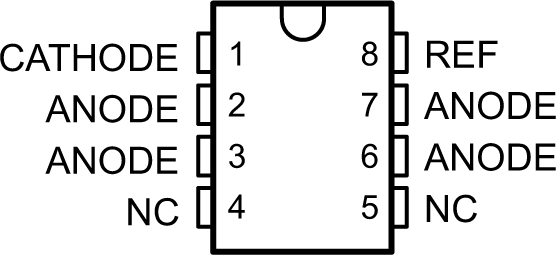
 Figure 4-1 D (SOIC) Package
 (Top View)
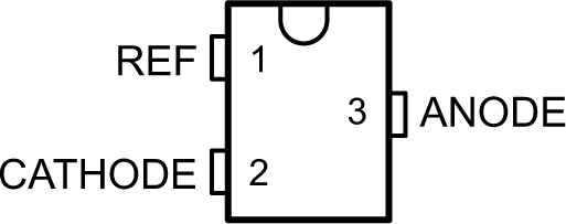
 Figure 4-3 DBZ (SOT-23-3) Package
(Top View)
 Figure 4-5 DCK (SC-70) Package
(Top View)

NC − No internal connection
* Pin 2 is attached to Substrate and must be connected to ANODE or left open.
Figure 4-2 DBV (SOT-23-5) Package(Top View)
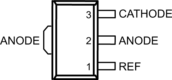
 Figure 4-4 PK (SOT-89) Package
 (Top View)
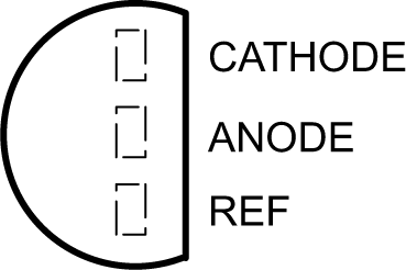
 Figure 4-6 LP (TO-92/TO-226) Package
(Top View)
Table 4-1 Pin Functions
| PIN | TYPE | DESCRIPTION | ||||||
|---|---|---|---|---|---|---|---|---|
| NAME | DBZ | DBV | PK | D | LP | DCK | ||
| CATHODE | 2 | 3 | 3 | 1 | 1 | 1 | I/O | Shunt Current/Voltage input |
| REF | 1 | 4 | 1 | 8 | 3 | 3 | I | Threshold relative to common anode |
| ANODE | 3 | 5 | 2 | 2, 3, 6, 7 | 2 | 6 | O | Common pin, normally connected to ground |
| NC | — | 1 | — | 4, 5 | — | 4, 5 | I | No Internal Connection |
| * | — | 2 | — | — | — | 2 | I | Substrate Connection. Must be connected to ANODE or left open. |