SLVS905B December 2008 – July 2024 TLV431A-Q1 , TLV431B-Q1
PRODUCTION DATA
- 1
- 1 Features
- 2 Applications
- 3 Description
- 4 Pin Configuration and Functions
- 5 Specifications
- 6 Parameter Measurement Information
- 7 Detailed Description
- 8 Applications and Implementation
- 9 Device and Documentation Support
- 10Revision History
- 11Mechanical, Packaging, and Orderable Information
Package Options
Mechanical Data (Package|Pins)
Thermal pad, mechanical data (Package|Pins)
Orderable Information
8.1 Application Information
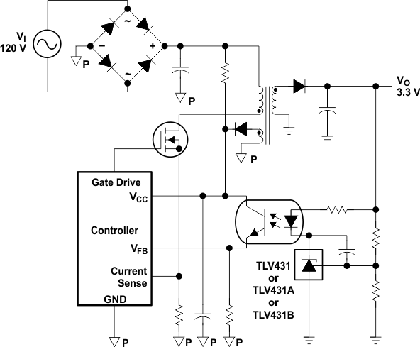
Figure 8-1 shows the TLV431A, or TLV431B used in a 3.3V isolated flyback supply. Output voltage VO can be as low as reference voltage VREF (1.24V ± 1%). The output of the regulator, plus the forward voltage drop of the optocoupler LED (1.24 + 1.4 = 2.64 V), determine the minimum voltage that can be regulated in an isolated supply configuration. Regulated voltage as low as 2.7Vdc is possible in the topology shown in Figure 8-1.
The 431 family of devices are prevalent in these applications, being designers go to choice for secondary side regulation. Due to this prevalence, this section explains the operation and design in both states of TLV431 that this application sees, open loop (Comparator + Vref) & closed loop (Shunt Regulator).
Further information about system stability and using a TLV431 device for compensation can be found in the application note Compensation Design With TL431 for UCC28600, SLUA671.
 Figure 8-1 Flyback With Isolation Using TLV431, TLV431A, or TLV431B as Voltage Reference and Error Amplifier