SLVS905B December 2008 – July 2024 TLV431A-Q1 , TLV431B-Q1
PRODUCTION DATA
- 1
- 1 Features
- 2 Applications
- 3 Description
- 4 Pin Configuration and Functions
- 5 Specifications
- 6 Parameter Measurement Information
- 7 Detailed Description
- 8 Applications and Implementation
- 9 Device and Documentation Support
- 10Revision History
- 11Mechanical, Packaging, and Orderable Information
Package Options
Mechanical Data (Package|Pins)
Thermal pad, mechanical data (Package|Pins)
Orderable Information
5.7 Typical Characteristics
Operation of the device at these or any other conditions beyond those indicated in the Section 5.4 table are not implied.
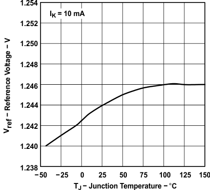 Figure 5-1 Reference Voltage vs Junction Temperature
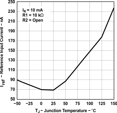 Figure 5-3 Reference Input Current vs Junction Temperature (for TLV431B)
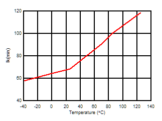 Figure 5-5 Minimum Cathode Current (µA) vs Temperature
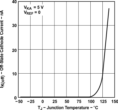 Figure 5-7 Off-State Cathode Current vs Junction Temperature for TLV431A
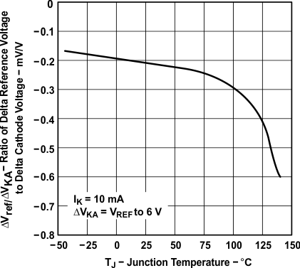 Figure 5-9 Ratio of Delta Reference Voltage to Delta Cathode Voltage vs Junction Temperature for TLV431A
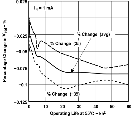
| ‡ Extrapolated from life-test data taken at 125°C; the activation energy assumed is 0.7 eV. |
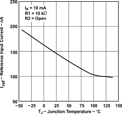 Figure 5-2 Reference Current vs Free- air Temperature (TLV431A)
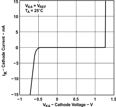 Figure 5-4 Cathode Current vs Cathode Voltage
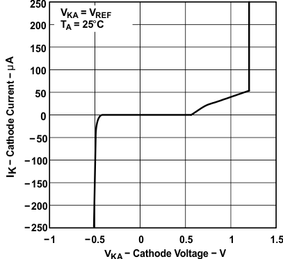 Figure 5-6 Cathode Current vs Cathode Voltage
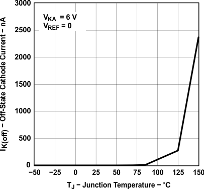 Figure 5-8 Off-State Cathode Current vs Junction Temperature for TLV431B
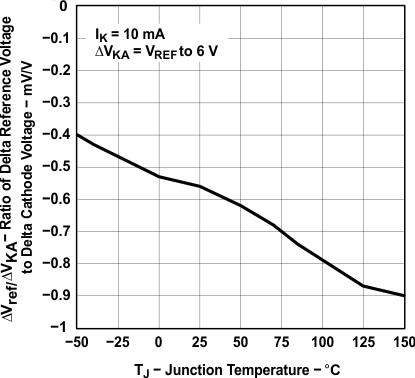 Figure 5-10 Ratio of Delta Reference Voltage to Delta Cathode Voltage vs Junction Temperature (for TLV431B)
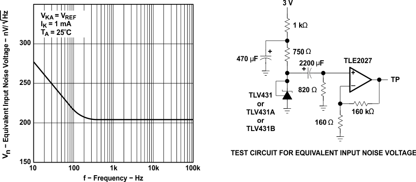 Figure 5-12 Equivalent Input Noise Voltage
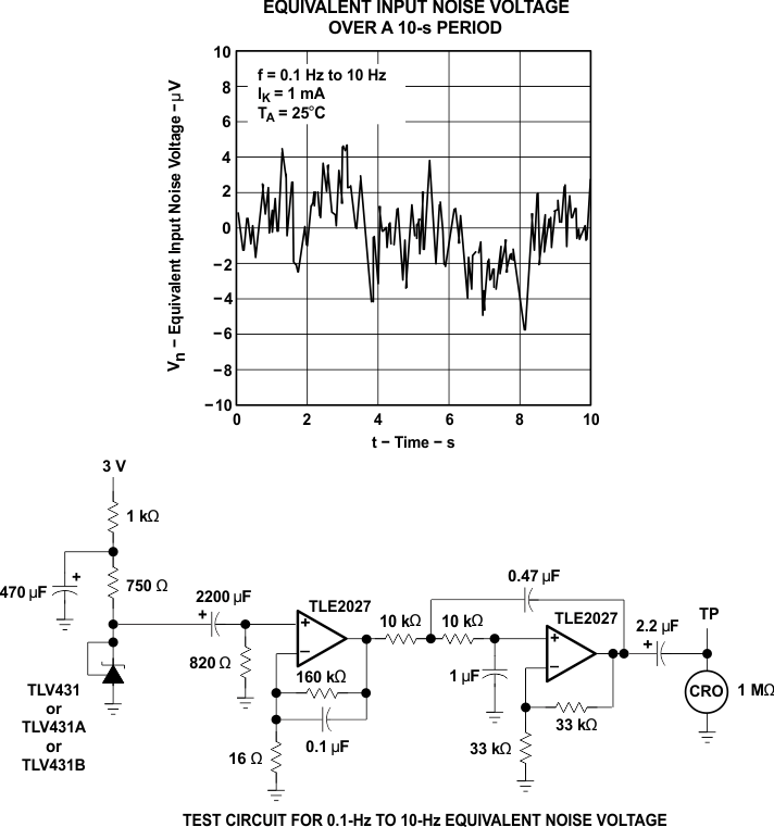 Figure 5-13 Equivalent Noise Voltage over a 10s Period
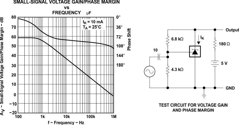 Figure 5-14 Voltage Gain and Phase Margin
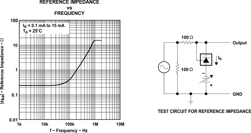 Figure 5-15 Reference Impedance vs Frequency
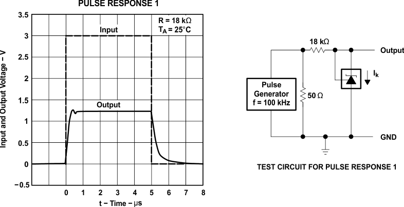 Figure 5-16 Pulse
Response 1
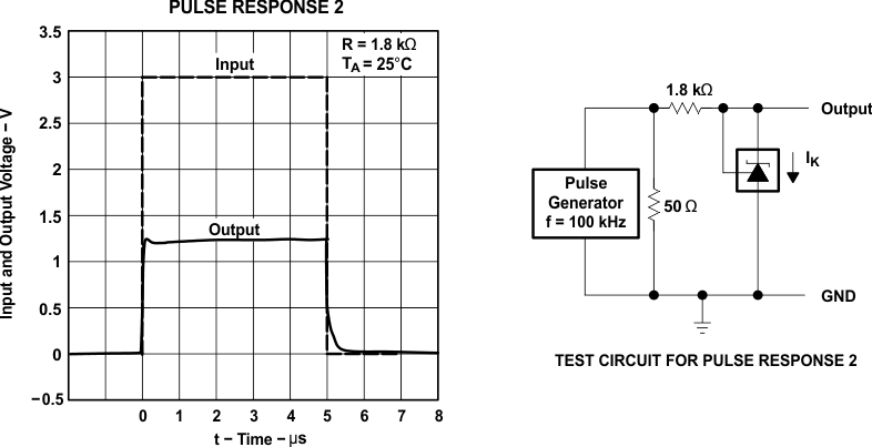 Figure 5-17 Pulse
Response 2
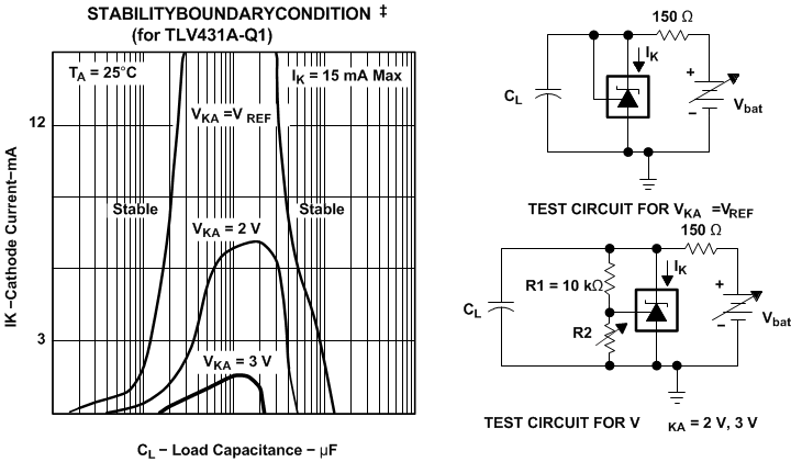
‡
The areas under the curves represent conditions that can cause the device to
oscillate. For VKA = 2V and 3V curves, R2 and Vbat
were adjusted to establish the initial VKA and IK
conditions with CL = 0. Vbat and CL then
were adjusted to determine the ranges of stability.
Figure 5-18 Stability Boundary Conditions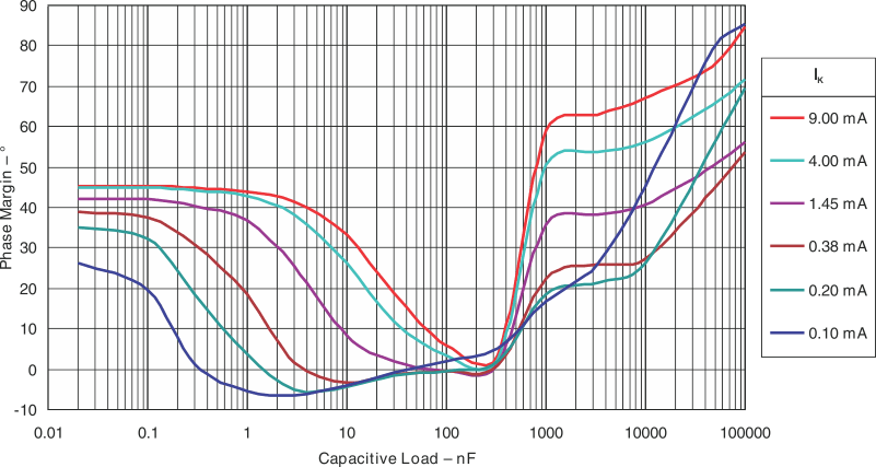 Figure 5-19 Phase
Margin vs Capacitive Load VKA = VREF (1.25 V),
TA= 25°C (For TLV431B-Q1)
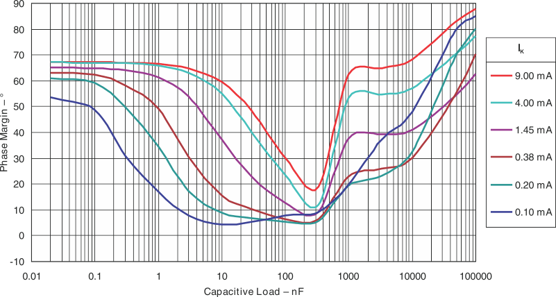 Figure 5-20 Phase
Margin vs Capacitive Load VKA = 2.50V, TA= 25°C (For
TLV431B-Q1)
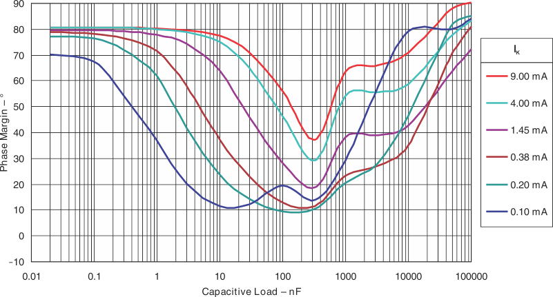 Figure 5-21 Phase
Margin vs Capacitive Load VKA = 5.00V, TA= 25°C (For
TLV431B-Q1)