SNOSDF0 May   2024 TLV4H290-SEP , TLV4H390-SEP

ADVANCE INFORMATION  

  1.   1
  2. Features
  3. Applications
  4. Description
  5. Pin Configuration and Functions
    1. 4.1 Pin Functions:TLV4H290-SEP and TLV4H390-SEP Quad
  6. Specifications
    1. 5.1 Absolute Maximum Ratings
    2. 5.2 ESD Ratings
    3. 5.3 Recommended Operating Conditions
    4. 5.4 Thermal Information, Quad
    5. 5.5 Electrical Characteristics, Quad
    6. 5.6 Switching Characteristics, Quad
    7. 5.7 Typical Characteristics
  7. Detailed Description
    1. 6.1 Overview
    2. 6.2 Functional Block Diagram
    3. 6.3 Feature Description
    4. 6.4 Device Functional Modes
      1. 6.4.1 Outputs
        1. 6.4.1.1 TLV4H290-SEP Open Drain Output
        2. 6.4.1.2 TLV4H390-SEP Push-Pull Output
      2. 6.4.2 Power-On Reset (POR)
      3. 6.4.3 Inputs
        1. 6.4.3.1 Rail to Rail Input
        2. 6.4.3.2 Fault Tolerant Inputs
        3. 6.4.3.3 Input Protection
      4. 6.4.4 ESD Protection
      5. 6.4.5 Unused Inputs
      6. 6.4.6 Hysteresis
  8. Application and Implementation
    1. 7.1 Application Information
      1. 7.1.1 Basic Comparator Definitions
        1. 7.1.1.1 Operation
        2. 7.1.1.2 Propagation Delay
        3. 7.1.1.3 Overdrive Voltage
      2. 7.1.2 Hysteresis
        1. 7.1.2.1 Inverting Comparator With Hysteresis
        2. 7.1.2.2 Non-Inverting Comparator With Hysteresis
        3. 7.1.2.3 Inverting and Non-Inverting Hysteresis using Open-Drain Output
    2. 7.2 Typical Applications
      1. 7.2.1 Window Comparator
        1. 7.2.1.1 Design Requirements
        2. 7.2.1.2 Detailed Design Procedure
        3. 7.2.1.3 Application Curve
      2. 7.2.2 Square-Wave Oscillator
        1. 7.2.2.1 Design Requirements
        2. 7.2.2.2 Detailed Design Procedure
        3. 7.2.2.3 Application Curve
      3. 7.2.3 Adjustable Pulse Width Generator
      4. 7.2.4 Time Delay Generator
      5. 7.2.5 Logic Level Shifter
      6. 7.2.6 One-Shot Multivibrator
      7. 7.2.7 Bi-Stable Multivibrator
      8. 7.2.8 Zero Crossing Detector
      9. 7.2.9 Pulse Slicer
    3. 7.3 Power Supply Recommendations
    4. 7.4 Layout
      1. 7.4.1 Layout Guidelines
      2. 7.4.2 Layout Example
  9. Device and Documentation Support
    1. 8.1 Documentation Support
      1. 8.1.1 Related Documentation
    2. 8.2 Receiving Notification of Documentation Updates
    3. 8.3 Support Resources
    4. 8.4 Trademarks
    5. 8.5 Electrostatic Discharge Caution
    6. 8.6 Glossary
  10. Revision History
  11. 10Mechanical, Packaging, and Orderable Information

Package Options

Mechanical Data (Package|Pins)
Thermal pad, mechanical data (Package|Pins)
Orderable Information

Inverting Comparator With Hysteresis

The inverting comparator with hysteresis requires a three-resistor network that is referenced to the comparator supply voltage (V+), as shown in Figure 7-3.

TLV4H290-SEP TLV4H390-SEP TLV4H390-SEP in an Inverting Configuration With HysteresisFigure 7-3 TLV4H390-SEP in an Inverting Configuration With Hysteresis

The equivalent resistor networks when the output is high and low are shown in Figure 7-3.

TLV4H290-SEP TLV4H390-SEP Inverting Configuration Resistor Equivalent NetworksFigure 7-4 Inverting Configuration Resistor Equivalent Networks

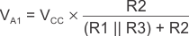
When VIN is less than VA, the output voltage is high (for simplicity, assume VO switches as high as VCC). The three network resistors can be represented as R1 || R3 in series with R2, as shown in Figure 7-4.

Equation 1 below defines the high-to-low trip voltage (VA1).

Equation 1. TLV4H290-SEP TLV4H390-SEP

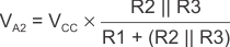
When VIN is greater than VA, the output voltage is low. In this case, the three network resistors can be presented as R2 || R3 in series with R1, as shown in Equation 2.

Use Equation 2 to define the low to high trip voltage (VA2).

Equation 2. TLV4H290-SEP TLV4H390-SEP

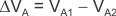
Equation 3 defines the total hysteresis provided by the network.

Equation 3. TLV4H290-SEP TLV4H390-SEP