SNOSDF0 May   2024 TLV4H290-SEP , TLV4H390-SEP

ADVANCE INFORMATION  

  1.   1
  2. Features
  3. Applications
  4. Description
  5. Pin Configuration and Functions
    1. 4.1 Pin Functions:TLV4H290-SEP and TLV4H390-SEP Quad
  6. Specifications
    1. 5.1 Absolute Maximum Ratings
    2. 5.2 ESD Ratings
    3. 5.3 Recommended Operating Conditions
    4. 5.4 Thermal Information, Quad
    5. 5.5 Electrical Characteristics, Quad
    6. 5.6 Switching Characteristics, Quad
    7. 5.7 Typical Characteristics
  7. Detailed Description
    1. 6.1 Overview
    2. 6.2 Functional Block Diagram
    3. 6.3 Feature Description
    4. 6.4 Device Functional Modes
      1. 6.4.1 Outputs
        1. 6.4.1.1 TLV4H290-SEP Open Drain Output
        2. 6.4.1.2 TLV4H390-SEP Push-Pull Output
      2. 6.4.2 Power-On Reset (POR)
      3. 6.4.3 Inputs
        1. 6.4.3.1 Rail to Rail Input
        2. 6.4.3.2 Fault Tolerant Inputs
        3. 6.4.3.3 Input Protection
      4. 6.4.4 ESD Protection
      5. 6.4.5 Unused Inputs
      6. 6.4.6 Hysteresis
  8. Application and Implementation
    1. 7.1 Application Information
      1. 7.1.1 Basic Comparator Definitions
        1. 7.1.1.1 Operation
        2. 7.1.1.2 Propagation Delay
        3. 7.1.1.3 Overdrive Voltage
      2. 7.1.2 Hysteresis
        1. 7.1.2.1 Inverting Comparator With Hysteresis
        2. 7.1.2.2 Non-Inverting Comparator With Hysteresis
        3. 7.1.2.3 Inverting and Non-Inverting Hysteresis using Open-Drain Output
    2. 7.2 Typical Applications
      1. 7.2.1 Window Comparator
        1. 7.2.1.1 Design Requirements
        2. 7.2.1.2 Detailed Design Procedure
        3. 7.2.1.3 Application Curve
      2. 7.2.2 Square-Wave Oscillator
        1. 7.2.2.1 Design Requirements
        2. 7.2.2.2 Detailed Design Procedure
        3. 7.2.2.3 Application Curve
      3. 7.2.3 Adjustable Pulse Width Generator
      4. 7.2.4 Time Delay Generator
      5. 7.2.5 Logic Level Shifter
      6. 7.2.6 One-Shot Multivibrator
      7. 7.2.7 Bi-Stable Multivibrator
      8. 7.2.8 Zero Crossing Detector
      9. 7.2.9 Pulse Slicer
    3. 7.3 Power Supply Recommendations
    4. 7.4 Layout
      1. 7.4.1 Layout Guidelines
      2. 7.4.2 Layout Example
  9. Device and Documentation Support
    1. 8.1 Documentation Support
      1. 8.1.1 Related Documentation
    2. 8.2 Receiving Notification of Documentation Updates
    3. 8.3 Support Resources
    4. 8.4 Trademarks
    5. 8.5 Electrostatic Discharge Caution
    6. 8.6 Glossary
  10. Revision History
  11. 10Mechanical, Packaging, and Orderable Information

Package Options

Mechanical Data (Package|Pins)
Thermal pad, mechanical data (Package|Pins)
Orderable Information

Detailed Design Procedure

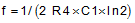
The oscillation frequency is determined by the resistor and capacitor values. The following calculation provides details of the steps.

TLV4H290-SEP TLV4H390-SEP Square-Wave Oscillator Timing ThresholdsFigure 7-10 Square-Wave Oscillator Timing Thresholds

First consider the output of Figure Figure 7-9 as high, which indicates the inverted input VC is lower than the noninverting input (VA). This causes the C1 to be charged through R4, and the voltage VC increases until it is equal to the noninverting input. The value of VA at the point is calculated by Equation 7.

Equation 7. TLV4H290-SEP TLV4H390-SEP

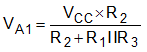
if R1 = R2= R3, then VA1 = 2VCC/ 3

At this time the comparator output trips pulling down the output to the negative rail. The value of VAat this point is calculated by Equation 8.

Equation 8. TLV4H290-SEP TLV4H390-SEP

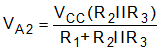
if R1 = R2 = R3, then VA2 = VCC/3

The C1 now discharges though the R4, and the voltage VCC decreases until it reaches VA2. At this point, the output switches back to the starting state. The oscillation period equals to the time duration from for C1 from 2VCC/3 to VCC / 3 then back to 2VCC/3, which is given by R4C1 × ln 2 for each trip. Therefore, the total time duration is calculated as 2 R4C1 × ln 2.

The oscillation frequency can be obtained by Equation 9:

Equation 9. TLV4H290-SEP TLV4H390-SEP