SNOSDA5D May 2020 – February 2023 TLV7031-Q1 , TLV7032-Q1 , TLV7034-Q1 , TLV7041-Q1 , TLV7042-Q1 , TLV7044-Q1
PRODUCTION DATA
- 1 Features
- 2 Applications
- 3 Description
- 4 Revision History
- 5 Pin Configuration and Functions
-
6 Specifications
- 6.1 Absolute Maximum Ratings
- 6.2 ESD Ratings
- 6.3 Recommended Operating Conditions
- 6.4 Thermal Information (Single)
- 6.5 Thermal Information (Dual)
- 6.6 Thermal Information (Quad)
- 6.7 Electrical Characteristics
- 6.8 Switching Characteristics
- 6.9 Electrical Characteristics (Dual)
- 6.10 Switching Characteristics (Dual)
- 6.11 Electrical Characteristics (Quad)
- 6.12 Switching Characteristics (Quad)
- 6.13 Timing Diagrams
- 6.14 Typical Characteristics
- 7 Detailed Description
- 8 Application and Implementation
- 9 Power Supply Recommendations
- 10Layout
- 11Device and Documentation Support
- 12Mechanical, Packaging, and Orderable Information
Package Options
Mechanical Data (Package|Pins)
- PW|14
Thermal pad, mechanical data (Package|Pins)
Orderable Information
7.4.2 Internal Hysteresis
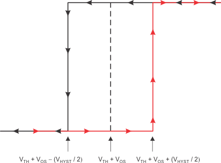
The device hysteresis transfer curve is shown in Figure 7-1. This curve is a function of three components: VTH, VOS, and VHYST:
- VTH is the actual set voltage or threshold trip voltage.
- VOS is the internal offset voltage between VIN+ and VIN–. This voltage is added to VTH to form the actual trip point at which the comparator must respond to change output states.
- VHYST is the internal hysteresis (or
trip window) that is designed to reduce comparator sensitivity to noise
(7 mV for both TLV703x-Q1 and TLV704x-Q1).
 Figure 7-1 Hysteresis Transfer Curve