6 Specifications
6.1 Absolute Maximum Ratings
over operating junction temperature range (unless otherwise noted)(1)
|
MIN |
MAX |
UNIT |
| Voltage(2) |
IN |
–0.3 |
6 |
V |
| EN |
–0.3 |
6 |
V |
| OUT |
–0.3 |
6 |
V |
| Current (source) |
OUT |
Internally limited |
|
| Output short-circuit duration |
Indefinite |
|
| Operating junction, TJ |
–55 |
150 |
°C |
| Storage, Tstg |
–55 |
150 |
°C |
(1) Stresses beyond those listed under Absolute Maximum Ratings may cause permanent damage to the device. These are stress ratings only, and functional operation of the device at these or any other conditions beyond those indicated under Recommended Operating Conditions is not implied. Exposure to absolute-maximum-rated conditions for extended periods my affect device reliability.
(2) All voltages are with respect to GND pin.
6.2 ESD Ratings
|
VALUE |
UNIT |
| V(ESD) |
Electrostatic discharge |
Human body model (HBM) QSS 009-105 (JESD22-A114A)(1) |
±2000 |
V |
| Charged device model (CDM) QSS 009-147 (JESD22-C101B.01)(2) |
±500 |
(1) JEDEC document JEP155 states that 500-V HBM allows safe manufacturing with a standard ESD control process.
(2) JEDEC document JEP157 states that 250-V CDM allows safe manufacturing with a standard ESD control process.
6.3 Recommended Operating Conditions
over operating junction temperature range (unless otherwise noted)
|
MIN |
NOM |
MAX |
UNIT |
| VIN |
Input voltage |
2 |
|
5.5 |
V |
| IOUT |
Output current |
0 |
|
200 |
mA |
| TJ |
Operating junction temperature range |
–40 |
|
125 |
°C |
6.4 Thermal Information
| THERMAL METRIC(1) |
TLV742P |
UNIT |
| DQN (X2SON) |
| 4 PINS |
| RθJA |
Junction-to-ambient thermal resistance |
180.4 |
°C/W |
| RθJC(top) |
Junction-to-case (top) thermal resistance |
152 |
°C/W |
| RθJB |
Junction-to-board thermal resistance |
117.2 |
°C/W |
| ψJT |
Junction-to-top characterization parameter |
5.1 |
°C/W |
| ψJB |
Junction-to-board characterization parameter |
117 |
°C/W |
| RθJC(bot) |
Junction-to-case (bottom) thermal resistance |
99.7 |
°C/W |
6.5 Electrical Characteristics
at VIN = VOUT(NOM) + 0.5 V or 2 V (whichever is greater); IOUT = 1 mA, VEN = VIN, COUT = 0.47 μF, and TJ = –40°C to +85°C. Typical values are at TJ = 25°C, (unless otherwise noted)
| PARAMETER |
TEST CONDITIONS |
MIN |
TYP |
MAX |
UNIT |
| VIN |
Input voltage range |
|
2 |
|
5.5 |
V |
| VOUT |
Output voltage range |
|
0.85 |
|
5 |
V |
| DC output accuracy |
|
|
0.5% |
|
|
| VOUT ≥ 0.85 V |
–1.5% |
|
1.5% |
|
| ΔVO(ΔVI) |
Line regulation |
|
|
1 |
5 |
mV |
| ΔVO(ΔIO) |
Load regulation |
0 mA ≤ IOUT ≤ 150 mA |
|
10 |
20 |
mV |
| V(DO) |
Dropout voltage |
VIN = 0.98 × VOUT(NOM) |
2 V < VOUT ≤ 2.4 V |
IOUT = 30 mA |
|
65 |
|
mV |
| IOUT = 150 mA |
|
325 |
360 |
mV |
| 2.4 V < VOUT ≤ 2.8 V |
IOUT = 30 mA |
|
50 |
|
mV |
| IOUT = 150 mA |
|
250 |
300 |
mV |
| 2.8 V < VOUT ≤ 3.3 V |
IOUT = 30 mA |
|
45 |
|
mV |
| IOUT = 150 mA |
|
220 |
270 |
mV |
| 3.3 V < VOUT ≤ 5 V |
IOUT = 30 mA |
|
40 |
|
mV |
| IOUT = 150 mA |
|
200 |
250 |
mV |
| ICL |
Output current limit |
VOUT = 0.9 × VOUT(NOM) |
240 |
300 |
450 |
mA |
| I(GND) |
Ground pin current |
IOUT = 0 mA |
|
25 |
50 |
µA |
| I(EN) |
EN pin current |
VEN = 5.5 V |
|
0.01 |
|
µA |
| ISHUTDOWN |
Shutdown current |
VEN ≤ 0.4 V
2 V ≤ VIN ≤ 4.5 V |
|
1 |
|
µA |
| VIL(EN) |
EN pin low-level input voltage
(disable device) |
|
0 |
|
0.4 |
V |
| VIH(EN) |
EN pin high-level input voltage (enable device) |
|
0.9 |
|
VIN |
V |
| PSRR |
Power-supply rejection ratio |
VIN = 3.3 V
VOUT = 2.8 V
IOUT = 30 mA |
f = 100 Hz |
|
70 |
|
dB |
| f = 10 kHz |
|
55 |
|
| f = 1 MHz |
|
55 |
|
| Vn |
Output noise voltage |
BW = 100 Hz to 100 kHz,
VIN = 2.3 V
VOUT = 1.8 V
IOUT = 10 mA |
|
45 |
|
µVRMS |
| tSTR |
Startup time(1) |
COUT = 1 µF
IOUT = 150 mA |
|
100 |
|
µs |
| RPULLDOWN |
Pulldown resistance
(TLV742P only) |
|
|
120 |
|
Ω |
| TJ |
Operating junction temperature |
|
–40 |
|
125 |
°C |
(1) Start-up time = time from EN assertion to 0.98 × VOUT.
6.6 Typical Characteristics
at TJ = –40°C to +85°C, VIN = VOUT(NOM) + 0.5 V or 2 V (whichever is greater), IOUT = 10 mA, VEN = VIN, and COUT = 1 µF Typical values are at TJ = 25°C, (unless otherwise noted)
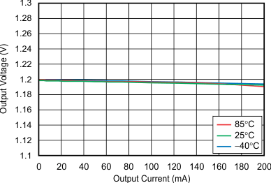
 Figure 1. Load Regulation

| VOUT = 1.2 V, IOUT = 10 mA |
Figure 3. Line Regulation

| VOUT = 1.2 V, IOUT = 150 mA |
Figure 5. Line Regulation
 Figure 7. Output Voltage vs Temperature
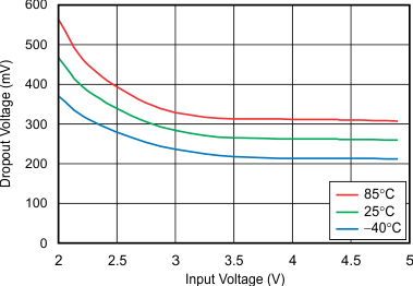
 Figure 9. Dropout Voltage vs Input Voltage
 Figure 11. Dropout Voltage vs Output Current

| VOUT = 2.8 V, IOUT = 0 mA |
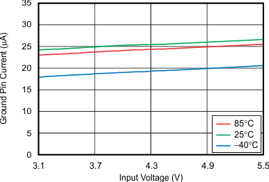
Figure 13. Ground Pin Current vs Input Voltage

| VOUT = 2.8 V, IOUT = 0 mA |
Figure 15. Ground Pin Current vs Temperature
 Figure 17. Ground Pin Current vs Output Current
 Figure 19. Shutdown Current vs Input Voltage
 Figure 21. Current Limit vs Input Voltage
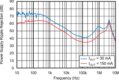
 Figure 23. Power-Supply Ripple Rejection vs Frequency

| VOUT = 2.8 V, IOUT = 150 mA |
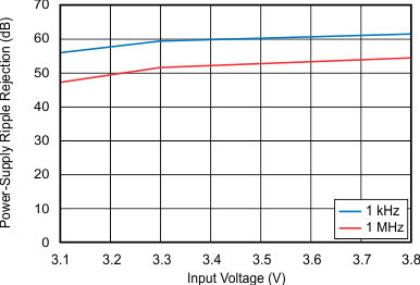
Figure 25. Power-Supply Ripple Rejection vs Input Voltage

| VOUT = 3.3 V, IOUT = 150 mA |
Figure 27. Power-Supply Ripple Rejection vs Input Voltage
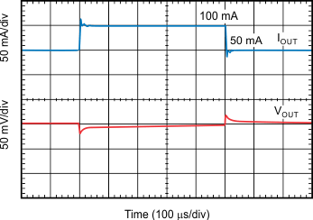
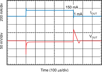
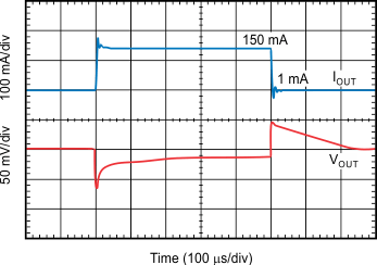
 Figure 29. Load Transient Response
 Figure 31. Load Transient Response

| VOUT = 1.2 V, IOUT = 150 mA |
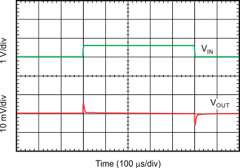
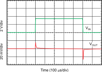
Figure 33. Line Transient Response

| VOUT = 1.2 V, IOUT = 150 mA |
Figure 35. Line Transient Response

| VOUT = 2.8 V, IOUT = 150 mA |
Figure 37. Line Transient Response

| VOUT = 2.8 V, IOUT = 200 mA |
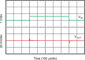
Figure 39. Line Transient Response

| VOUT = 1.2 V, IOUT = 30 mA |
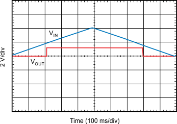
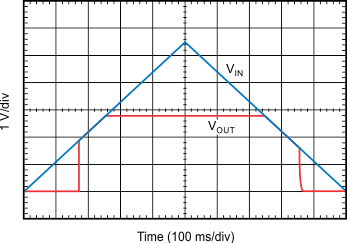
Figure 41. VIN Ramp Up, Ramp Down Response
 Figure 2. Load Regulation

| VOUT = 2.8 V, IOUT = 10 mA |
Figure 4. Line Regulation

| VOUT = 2.8 V, IOUT = 150 mA |
Figure 6. Line Regulation
 Figure 8. Output Voltage vs Temperature
 Figure 10. Dropout Voltage vs Input Voltage

| VOUT = 1.2 V, IOUT = 0 mA |
Figure 12. Ground Pin Current vs Input Voltage

| VOUT = 1.2 V, IOUT = 0 mA |
Figure 14. Ground Pin Current vs Temperature
 Figure 16. Ground Pin Current vs Output Current
 Figure 18. Shutdown Current vs Input Voltage
 Figure 20. Current Limit vs Input Voltage
 Figure 22. Power-Supply Ripple Rejection vs Frequency

| VOUT = 2.8 V, IOUT = 30 mA |
Figure 24. Power-Supply Ripple Rejection vs Input Voltage

| VOUT = 3.3 V, IOUT = 30 mA |
Figure 26. Power-Supply Ripple Rejection vs Input Voltage
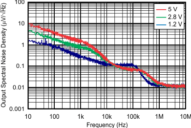
 Figure 28. Output Spectral Noise Density vs Frequency
 Figure 30. Load Transient Response
 Figure 32. Load Transient Response

| VOUT = 1.2 V, IOUT = 200 mA |
Figure 34. Line Transient Response

| VOUT = 1.2 V, IOUT = 200 mA |
Figure 36. Line Transient Response

| VOUT = 2.8 V, IOUT = 200 mA |
Figure 38. Line Transient Response

| VOUT = 2.8 V, IOUT = 200 mA |
Figure 40. Line Transient Response

| VOUT = 2.8 V, IOUT = 30 mA |
Figure 42. VIN Ramp Up, Ramp Down Response
