SBVS456A September   2024  – December 2024 TLV774

PRODUCTION DATA  

  1.   1
  2. Features
  3. Applications
  4. Description
  5. Pin Configuration and Functions
  6. Specifications
    1. 5.1 Absolute Maximum Ratings
    2. 5.2 ESD Ratings
    3. 5.3 Recommended Operating Conditions
    4. 5.4 Thermal Information
    5. 5.5 Electrical Characteristics
    6. 5.6 Switching Characteristics
    7. 5.7 Typical Characteristics
  7. Detailed Description
    1. 6.1 Overview
    2. 6.2 Functional Block Diagram
    3. 6.3 Feature Description
      1. 6.3.1 Dropout Voltage
      2. 6.3.2 Active Discharge
      3. 6.3.3 Foldback Current Limit
      4. 6.3.4 Thermal Shutdown
    4. 6.4 Device Functional Modes
      1. 6.4.1 Normal Operation
      2. 6.4.2 Dropout Operation
      3. 6.4.3 Disabled
  8. Application and Implementation
    1. 7.1 Application Information
      1. 7.1.1 Recommended Capacitor Types
      2. 7.1.2 Input and Output Capacitor Requirements
    2. 7.2 Typical Application
      1. 7.2.1 Application
      2. 7.2.2 Design Requirements
      3. 7.2.3 Detailed Design Procedure
      4. 7.2.4 Application Curves
    3. 7.3 Power Supply Recommendations
    4. 7.4 Layout
      1. 7.4.1 Layout Guidelines
      2. 7.4.2 Layout Example
  9. Device and Documentation Support
    1. 8.1 Device Support
      1. 8.1.1 Device Nomenclature
    2. 8.2 Documentation Support
      1. 8.2.1 Related Documentation
    3. 8.3 Receiving Notification of Documentation Updates
    4. 8.4 Support Resources
    5. 8.5 Trademarks
    6. 8.6 Electrostatic Discharge Caution
    7. 8.7 Glossary
  10. Revision History
  11. 10Mechanical, Packaging, and Orderable Information

Package Options

Mechanical Data (Package|Pins)
Thermal pad, mechanical data (Package|Pins)
Orderable Information

Typical Characteristics

at operating temperature TJ = 25°C, VIN = VOUT(NOM) + 0.5V, IOUT = 1mA, VEN = VIN, and CIN = COUT = 1μF (unless otherwise noted)
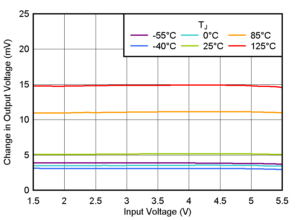
TLV774 Line Regulation vs VIN
 
Figure 5-1 Line Regulation vs VIN
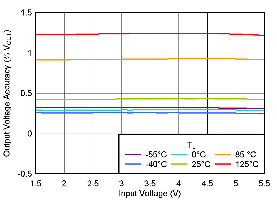
TLV774 Output Voltage Accuracy vs VIN
 
Figure 5-3 Output Voltage Accuracy vs VIN
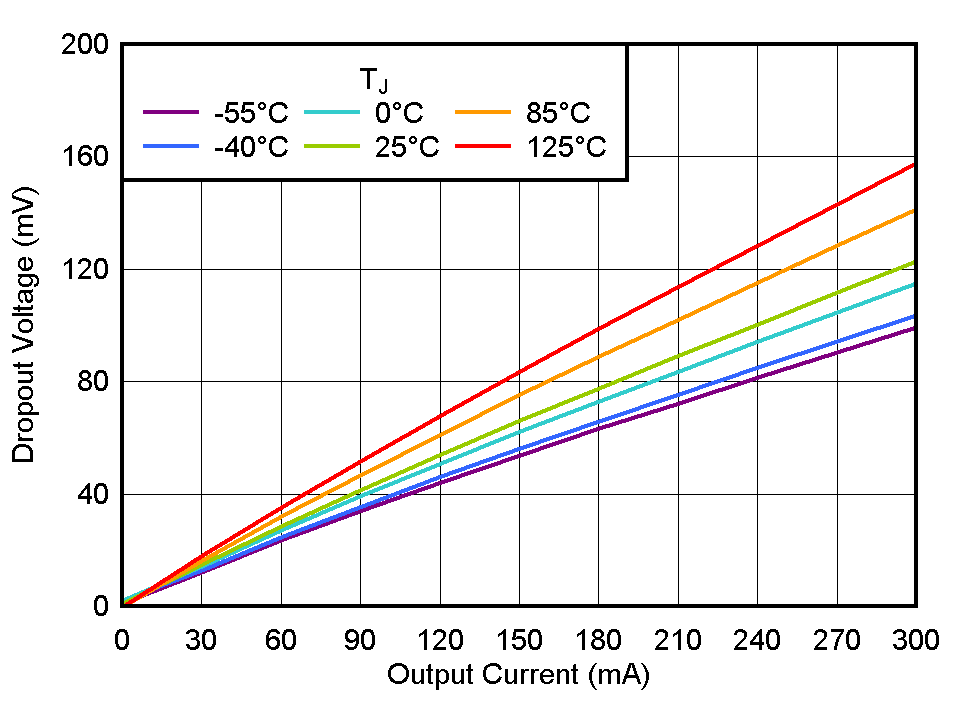
TLV774 Dropout Voltage vs IOUT
VOUT = 3.3V, Test condition: VIN = VOUT(NOM)
Figure 5-5 Dropout Voltage vs IOUT
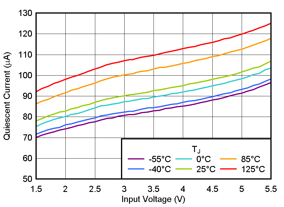
TLV774 Quiescent Current vs VIN
Figure 5-7 Quiescent Current vs VIN
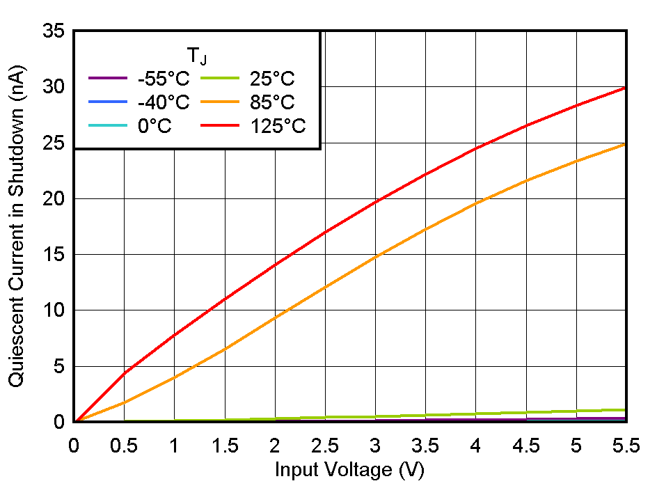
TLV774 Shutdown Current vs VIN
VEN = 0V, CIN= 0μF
Figure 5-9 Shutdown Current vs VIN
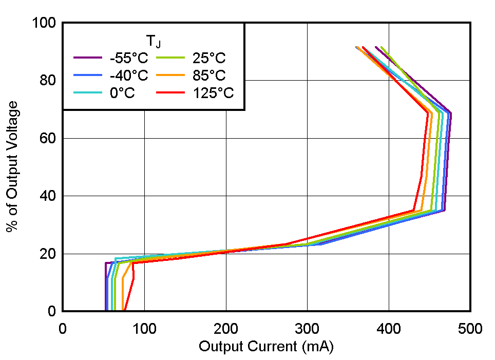
TLV774 Current Limit
 
Figure 5-11 Current Limit
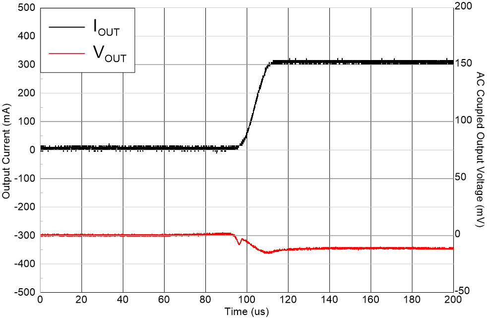
TLV774 Load
                        Transient
VIN = VOUT(nom) + 1.0V, IOUT = 0mA to 300mA,
TRISING = 10µs
Figure 5-13 Load Transient
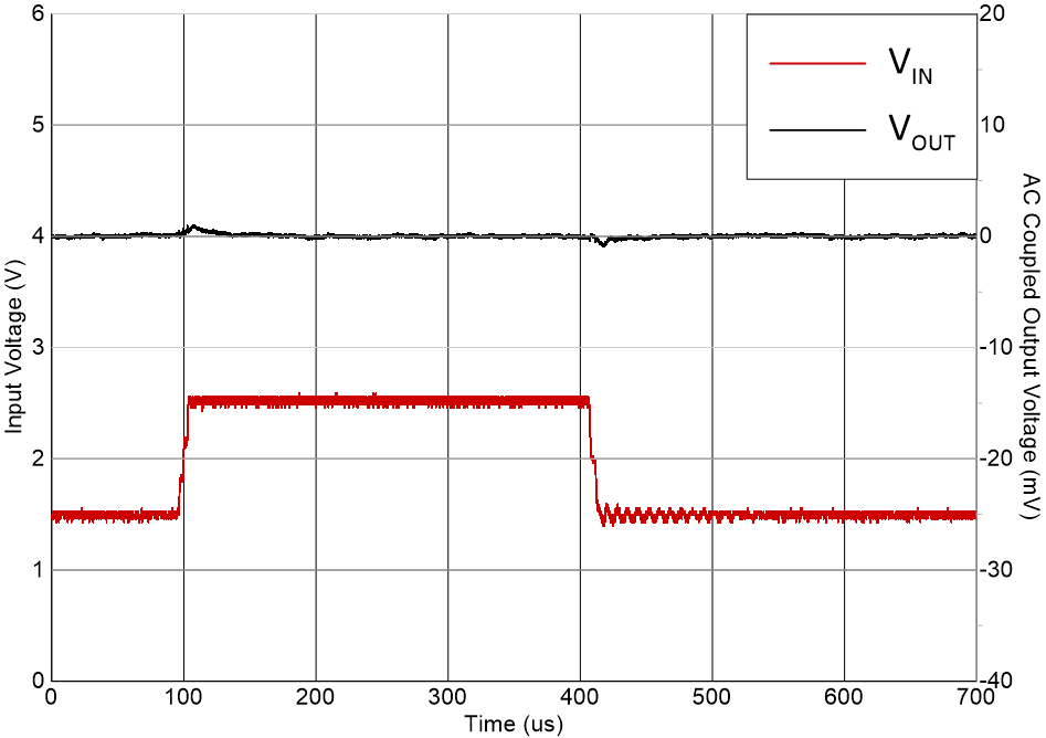
TLV774 Line
                        Transient
VIN = VOUT + 0.3V to VOUT +1.3V
Figure 5-15 Line Transient
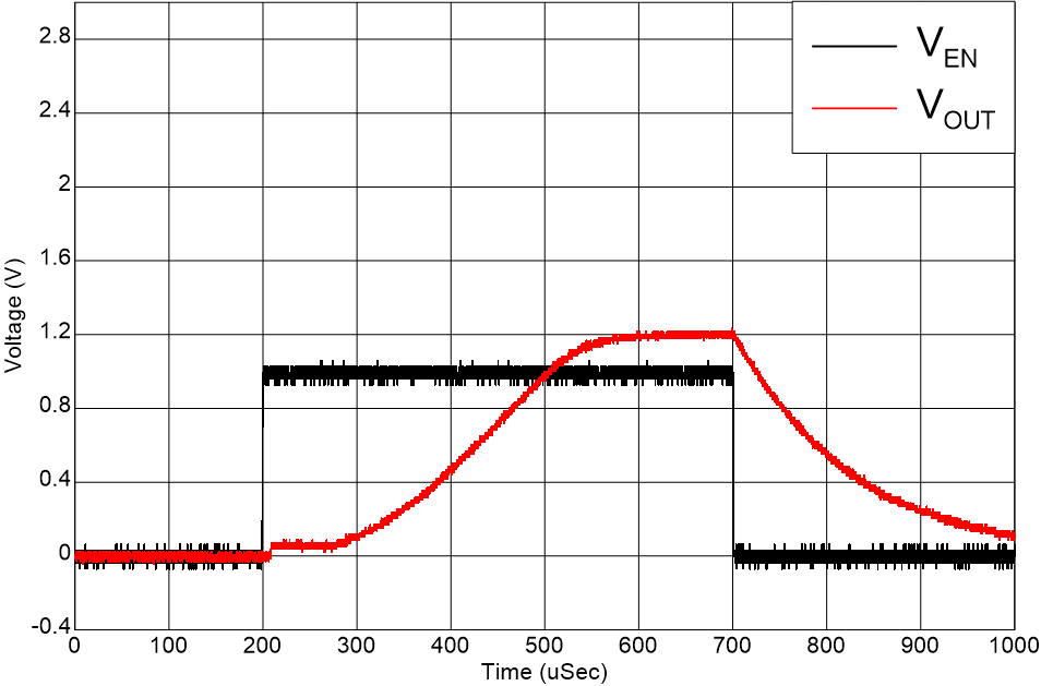
TLV774 Start-Up
 
Figure 5-17 Start-Up
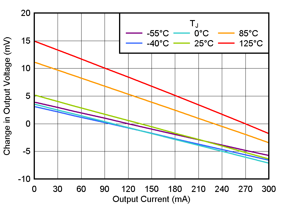
TLV774 Load
                        Regulation vs IOUT
 
Figure 5-2 Load Regulation vs IOUT
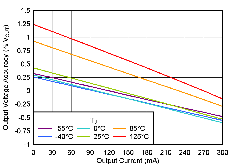
TLV774 Output Voltage Accuracy vs IOUT
 
Figure 5-4 Output Voltage Accuracy vs IOUT
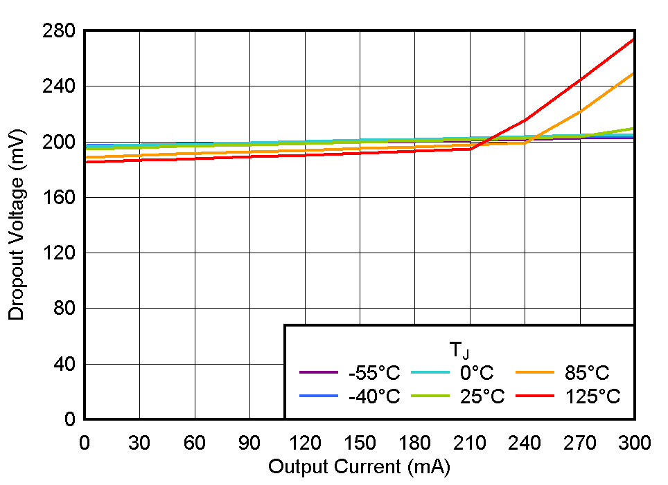
TLV774 Dropout Voltage vs IOUT
VOUT = 1.2V, Test condition: VIN = 1.4V
Figure 5-6 Dropout Voltage vs IOUT
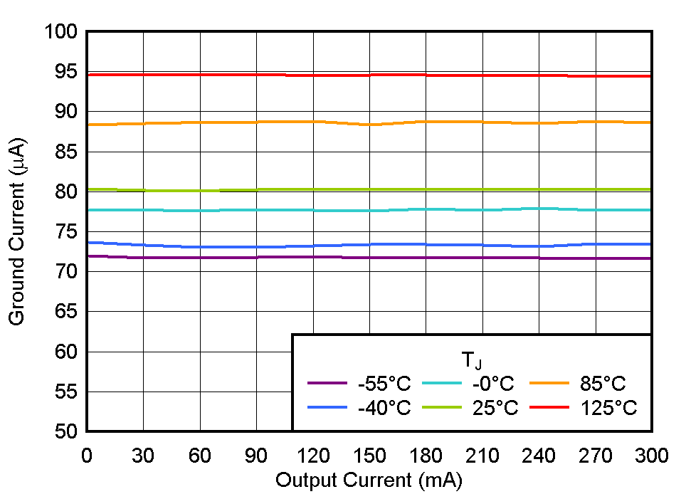
TLV774 Ground Current vs IOUT
 
Figure 5-8 Ground Current vs IOUT
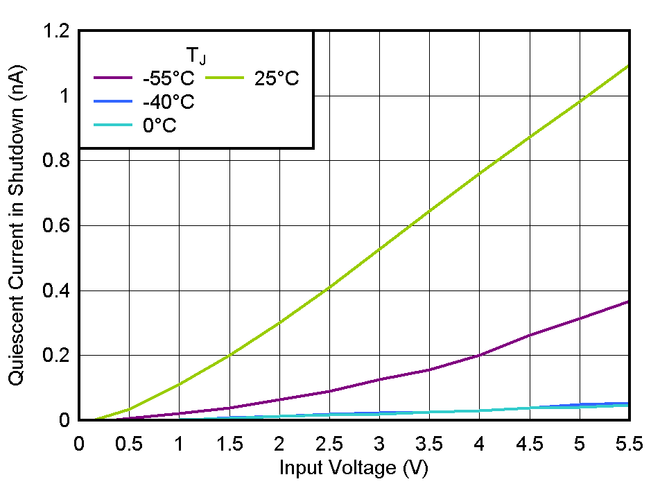
TLV774 Shutdown Current vs VIN
VEN = 0V, CIN= 0μF
Figure 5-10 Shutdown Current vs VIN
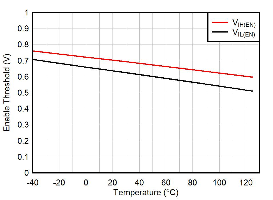
TLV774 Enable Logic Threshold vs Temperature
 
Figure 5-12 Enable Logic Threshold vs Temperature
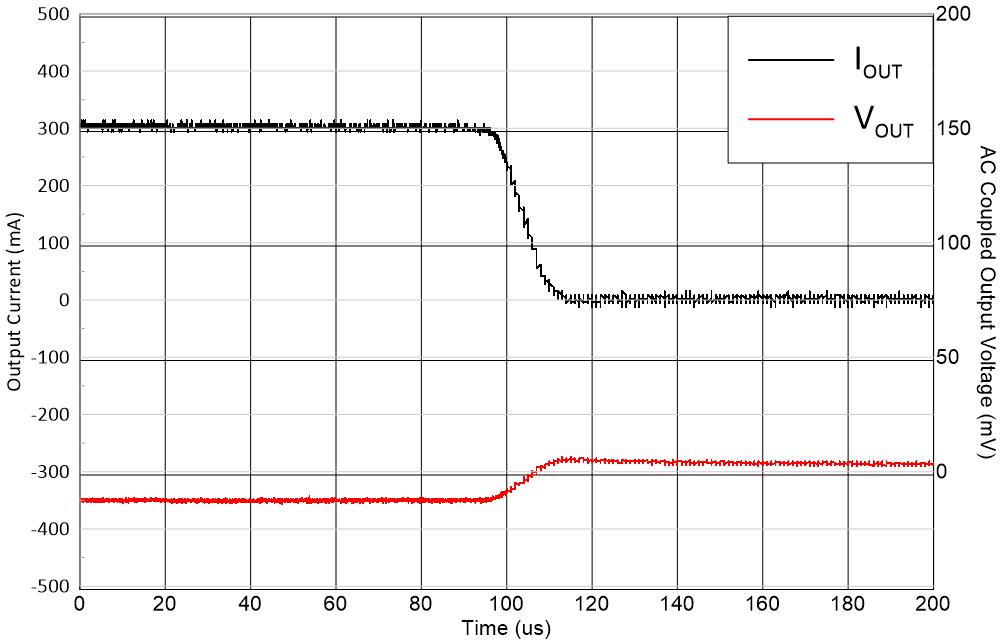
TLV774 Load
                        Transient
VIN = VOUT(nom) + 1.0V, IOUT = 300mA to 0mA,
TFALLING = 10µs
Figure 5-14 Load Transient
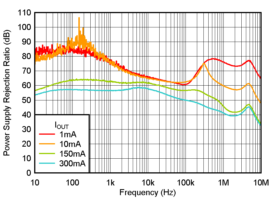
TLV774 PSRR
                        vs Frequency
VIN = VOUT(nom) + 1.0V
Figure 5-16 PSRR vs Frequency
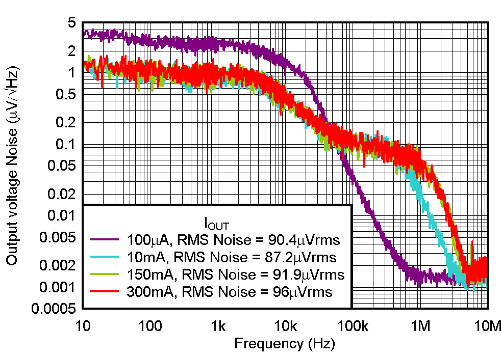
TLV774 Noise
VOUT = 1.2V, RMS Noise BW = 10Hz to 100kHz
Figure 5-18 Noise