SBOSAK0A June 2024 – August 2024 TLV9044-Q1
PRODMIX
- 1
- 1 Features
- 2 Applications
- 3 Description
- 4 Pin Configuration and Functions
- 5 Specifications
- 6 Detailed Description
- 7 Application and Implementation
- 8 Device and Documentation Support
- 9 Revision History
- 10Mechanical, Packaging, and Orderable Information
Package Options
Mechanical Data (Package|Pins)
- PW|14
Thermal pad, mechanical data (Package|Pins)
Orderable Information
3 Description
The low-power TLV904x-Q1 family includes single, dual, and quad-channel ultra-low-voltage (1.2V to 5.5V) operational amplifiers (op amps) with rail-to-rail input and output swing capabilities. The TLV904x-Q1 enables power savings both with the low quiescent current (10µA, typical) and the ability to operate at supply voltages as low as 1.2V. These devices are designed to be cost-effective for power and space-constrained applications where low-voltage operation is crucial.
The robust design of the TLV904x-Q1 family simplifies circuit design. These op amps feature an integrated RFI and EMI rejection filter, unity-gain stability, and no-phase reversal in input overdrive conditions. The device also delivers excellent AC performance with a gain bandwidth of 350kHz and a high capacitive load drive of 100pF, enabling designers to achieve both improved performance and lower power consumption.
| PART NUMBER(1) | CHANNEL COUNT | PACKAGE | PACKAGE SIZE (4) |
|---|---|---|---|
| TLV9041-Q1(2) | Single | DBV (SOT-23, 5) | 2.9mm × 2.80mm |
| DCK (SC70, 5) | 2.00mm × 2.10mm | ||
| TLV9042-Q1(2) | Dual | D (SOIC, 8) | 4.90mm × 6.00mm |
| DGK (VSSOP, 8) | 3.00mm × 4.90mm | ||
| PW (TSSOP, 8) | 3.00mm × 6.40mm | ||
| TLV9044-Q1 | Quad | D (SOIC, 14)(3) | 8.65mm × 6.00mm |
| PW (TSSOP, 14) | 5.00mm × 6.40mm | ||
| DYY (SOT-23, 14) (3) | 4.20mm × 3.26mm |
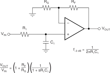
 Single-Pole, Low-Pass Filter