SBOS839M March   2017  – December 2024 TLV9061 , TLV9062 , TLV9064

PRODMIX  

  1.   1
  2. Features
  3. Applications
  4. Description
  5.   Device Comparison Table
  6. Pin Configuration and Functions
  7. Specifications
    1. 5.1  Absolute Maximum Ratings
    2. 5.2  ESD Ratings
    3. 5.3  Recommended Operating Conditions
    4. 5.4  Thermal Information: TLV9061
    5. 5.5  Thermal Information: TLV9061S
    6. 5.6  Thermal Information: TLV9062
    7. 5.7  Thermal Information: TLV9062S
    8. 5.8  Thermal Information: TLV9064
    9. 5.9  Thermal Information: TLV9064S
    10. 5.10 Electrical Characteristics
    11. 5.11 Typical Characteristics
  8. Detailed Description
    1. 6.1 Overview
    2. 6.2 Functional Block Diagram
    3. 6.3 Feature Description
      1. 6.3.1 Rail-to-Rail Input
      2. 6.3.2 Rail-to-Rail Output
      3. 6.3.3 EMI Rejection
      4. 6.3.4 Overload Recovery
      5. 6.3.5 Shutdown Function
    4. 6.4 Device Functional Modes
  9. Application and Implementation
    1. 7.1 Application Information
    2. 7.2 Typical Applications
      1. 7.2.1 Typical Low-Side Current Sense Application
      2. 7.2.2 Design Requirements
      3. 7.2.3 Detailed Design Procedure
      4. 7.2.4 Application Curve
    3. 7.3 Power Supply Recommendations
      1. 7.3.1 Input and ESD Protection
    4. 7.4 Layout
      1. 7.4.1 Layout Guidelines
      2. 7.4.2 Layout Example
  10. Device and Documentation Support
    1. 8.1 Documentation Support
      1. 8.1.1 Related Documentation
    2. 8.2 Receiving Notification of Documentation Updates
    3. 8.3 Support Resources
    4. 8.4 Trademarks
    5. 8.5 Electrostatic Discharge Caution
    6. 8.6 Glossary
  11. Revision History
  12. 10Mechanical, Packaging, and Orderable Information

Package Options

Mechanical Data (Package|Pins)
Thermal pad, mechanical data (Package|Pins)
Orderable Information

Typical Characteristics

at TA = 25°C, VS = 5.5V, RL = 10kΩ connected to VS / 2, VCM = VS / 2, and VOUT = VS / 2 (unless otherwise noted)
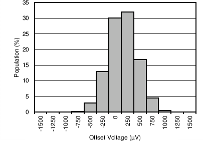
TLV9061 TLV9062 TLV9064 Offset Voltage Production Distribution
Figure 5-1 Offset Voltage Production Distribution
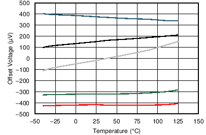
TLV9061 TLV9062 TLV9064 Offset Voltage vs Temperature
Figure 5-3 Offset Voltage vs Temperature
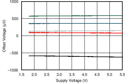
TLV9061 TLV9062 TLV9064 Offset Voltage vs Power Supply
VS = 1.8V to 5.5V
Figure 5-5 Offset Voltage vs Power Supply
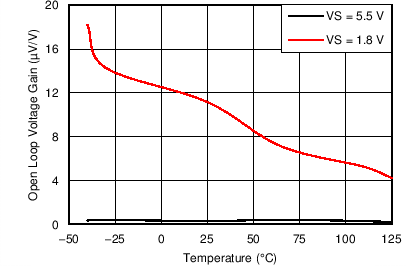
TLV9061 TLV9062 TLV9064 Open-Loop Gain vs Temperature
RL = 2kΩ
Figure 5-7 Open-Loop Gain vs Temperature
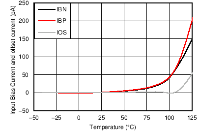
TLV9061 TLV9062 TLV9064 Input Bias Current vs Temperature
Figure 5-9 Input Bias Current vs Temperature
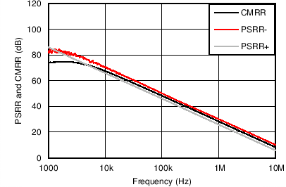
TLV9061 TLV9062 TLV9064 CMRR and PSRR vs Frequency  (Referred to Input)
Figure 5-11 CMRR and PSRR vs Frequency (Referred to Input)
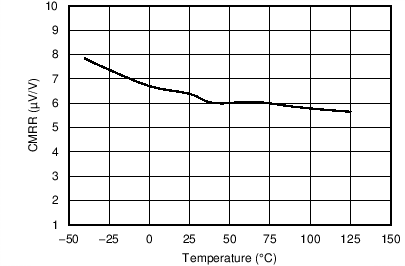
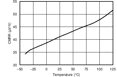
TLV9061 TLV9062 TLV9064 CMRR vs Temperature
VCM = (V–) – 0.1V to (V+) – 1.4V
TA= –40°C to 125°CRL= 10kΩVS = 5.5V
Figure 5-13 CMRR vs Temperature
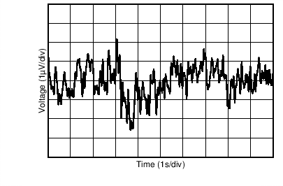
TLV9061 TLV9062 TLV9064 0.1Hz to 10Hz Input Voltage Noise
VS = 1.8V to 5.5V
Figure 5-15 0.1Hz to 10Hz Input Voltage Noise
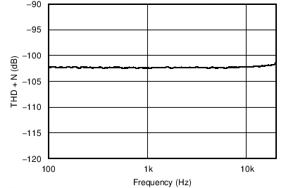
TLV9061 TLV9062 TLV9064 THD + N vs Frequency
VS = 5.5VVCM = 2.5VRL = 2kΩ
VOUT = 0.5VRMSBW = 80kHzG = +1
Figure 5-17 THD + N vs Frequency
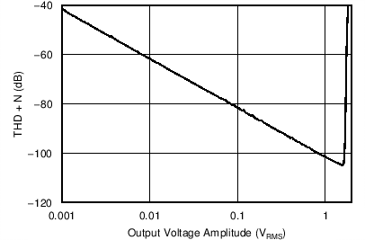
TLV9061 TLV9062 TLV9064 THD + N vs Amplitude
VS = 5.5VVCM = 2.5VRL = 2kΩ
G = –1BW = 80kHzf = 1kHz
Figure 5-19 THD + N vs Amplitude
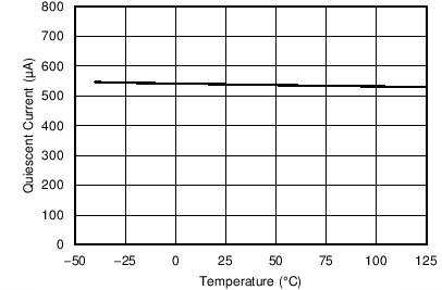
TLV9061 TLV9062 TLV9064 Quiescent Current vs Temperature
Figure 5-21 Quiescent Current vs Temperature
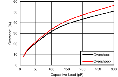
TLV9061 TLV9062 TLV9064 Small-Signal Overshoot vs Load Capacitance
V+ = 2.75VV– = –2.75VG = +1V/V
VOUT step = 100mVp-pRL = 10kΩ
Figure 5-23 Small-Signal Overshoot vs Load Capacitance
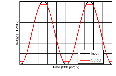
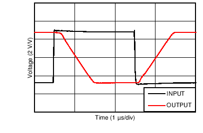
TLV9061 TLV9062 TLV9064 No Phase Reversal
V+ = 2.75VV– = –2.75V
Figure 5-25 No Phase Reversal
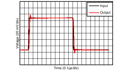
TLV9061 TLV9062 TLV9064 Small-Signal Step Response
V+ = 2.75VV– = –2.75VG = 1V/V
Figure 5-27 Small-Signal Step Response
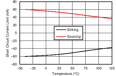
TLV9061 TLV9062 TLV9064 Short-Circuit Current vs Temperature
Figure 5-29 Short-Circuit Current vs Temperature
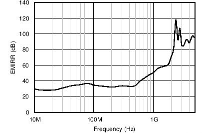
TLV9061 TLV9062 TLV9064 Electromagnetic Interference Rejection Ratio Referred to Noninverting Input (EMIRR+) vs Frequency
PRF = –10dBm
Figure 5-31 Electromagnetic Interference Rejection Ratio Referred to Noninverting Input (EMIRR+) vs Frequency
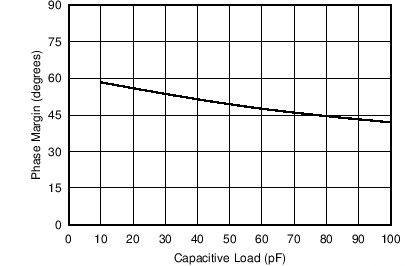
TLV9061 TLV9062 TLV9064 Phase Margin vs Capacitive Load
VS = 5.5V
Figure 5-33 Phase Margin vs Capacitive Load
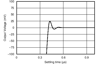
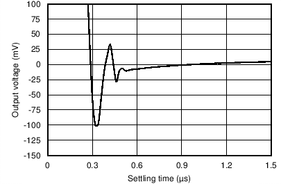
TLV9061 TLV9062 TLV9064 Large Signal Settling Time (Positive)
Figure 5-35 Large Signal Settling Time (Positive)
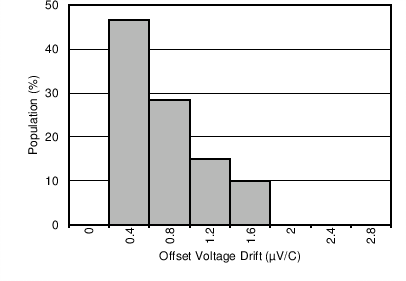
TLV9061 TLV9062 TLV9064 Offset Voltage Drift Distribution
TA = –40°C to 125°C
Figure 5-2 Offset Voltage Drift Distribution
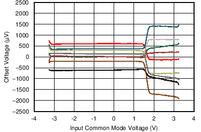
TLV9061 TLV9062 TLV9064 Offset Voltage vs Common-Mode Voltage
V+ = 2.75VV– = –2.75V
Figure 5-4 Offset Voltage vs Common-Mode Voltage
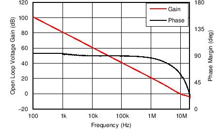
TLV9061 TLV9062 TLV9064 Open-Loop Gain and Phase vs Frequency
CL = 10pF
Figure 5-6 Open-Loop Gain and Phase vs Frequency
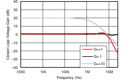
TLV9061 TLV9062 TLV9064 Closed-Loop Gain vs Frequency
Figure 5-8 Closed-Loop Gain vs Frequency
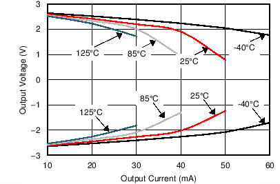
TLV9061 TLV9062 TLV9064 Output Voltage Swing vs Output Current
V+ = 2.75VV– = –2.75V
Figure 5-10 Output Voltage Swing vs Output Current
TLV9061 TLV9062 TLV9064 CMRR vs Temperature
VS = 5.5VVCM = –0.1V to 5.6VTA= –40°C to 125°C
RL= 10kΩ
Figure 5-12 CMRR vs Temperature
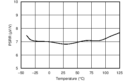
TLV9061 TLV9062 TLV9064 PSRR vs Temperature
VS = 1.8V to 5.5V
Figure 5-14 PSRR vs Temperature
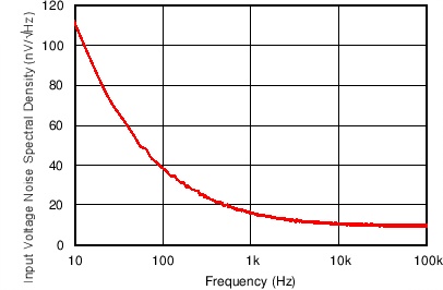
TLV9061 TLV9062 TLV9064 Input Voltage Noise Spectral Density vs Frequency
Figure 5-16 Input Voltage Noise Spectral Density vs Frequency
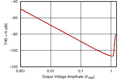
TLV9061 TLV9062 TLV9064 THD + N vs Amplitude
VS = 5.5VRL = 2kΩG = +1
VCM = 2.5VBW = 80kHzf = 1kHz
Figure 5-18 THD + N vs Amplitude
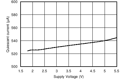
TLV9061 TLV9062 TLV9064 Quiescent Current vs Supply Voltage
Figure 5-20 Quiescent Current vs Supply Voltage
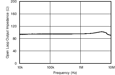
TLV9061 TLV9062 TLV9064 Open-Loop Output Impedance vs Frequency
Figure 5-22 Open-Loop Output Impedance vs Frequency
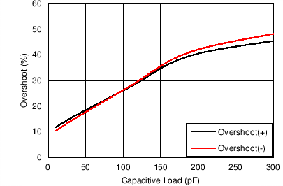
TLV9061 TLV9062 TLV9064 Small-Signal Overshoot vs Load Capacitance
V+ = 2.75VV– = –2.75VG = –1V/V
VOUT step = 100mVp-pRL = 10kΩ
Figure 5-24 Small-Signal Overshoot vs Load Capacitance
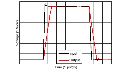
TLV9061 TLV9062 TLV9064 Overload Recovery
V+ = 2.75VV– = –2.75VG = –10V/V
Figure 5-26 Overload Recovery
TLV9061 TLV9062 TLV9064 Large-Signal Step Response
V+ = 2.75VV– = –2.75VCL = 100pF
G = 1V/V
Figure 5-28 Large-Signal Step Response
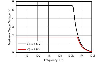
TLV9061 TLV9062 TLV9064 Maximum Output Voltage vs Frequency and Supply Voltage
RL = 10 k‎ΩCL = 10pF
Figure 5-30 Maximum Output Voltage vs Frequency and Supply Voltage
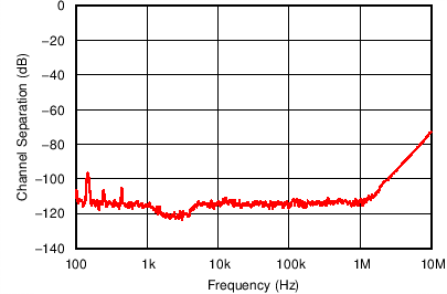
TLV9061 TLV9062 TLV9064 Channel Separation vs Frequency
V+ = 2.75VV– = –2.75V
Figure 5-32 Channel Separation vs Frequency
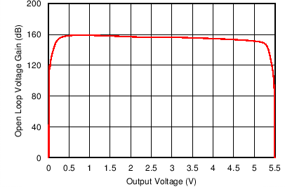
TLV9061 TLV9062 TLV9064 Open Loop Voltage Gain vs Output Voltage
VS = 5.5V
Figure 5-34 Open Loop Voltage Gain vs Output Voltage
TLV9061 TLV9062 TLV9064 Large Signal Settling Time (Negative)
Figure 5-36 Large Signal Settling Time (Negative)