SBOS839M March 2017 – December 2024 TLV9061 , TLV9062 , TLV9064
PRODMIX
- 1
- 1 Features
- 2 Applications
- 3 Description
- Device Comparison Table
- 4 Pin Configuration and Functions
-
5 Specifications
- 5.1 Absolute Maximum Ratings
- 5.2 ESD Ratings
- 5.3 Recommended Operating Conditions
- 5.4 Thermal Information: TLV9061
- 5.5 Thermal Information: TLV9061S
- 5.6 Thermal Information: TLV9062
- 5.7 Thermal Information: TLV9062S
- 5.8 Thermal Information: TLV9064
- 5.9 Thermal Information: TLV9064S
- 5.10 Electrical Characteristics
- 5.11 Typical Characteristics
- 6 Detailed Description
- 7 Application and Implementation
- 8 Device and Documentation Support
- 9 Revision History
- 10Mechanical, Packaging, and Orderable Information
Package Options
Mechanical Data (Package|Pins)
Thermal pad, mechanical data (Package|Pins)
- DPW|5
Orderable Information
4 Pin Configuration and Functions
 Figure 4-1 TLV9061 DBV or DRL Package,5-Pin SOT-23 or SOT-553(Top View)
 Figure 4-3 TLV9061 DPW Package,
5-Pin X2SON(Top View)
 Figure 4-2 TLV9061 DCK Package,5-Pin SC70(Top View)
Table 4-1 Pin Functions: TLV9061
| PIN | TYPE(1) | DESCRIPTION | |||
|---|---|---|---|---|---|
| NAME | SOT-23, SOT-553 |
SC70 | X2SON | ||
| IN– | 4 | 3 | 2 | I | Inverting input |
| IN+ | 3 | 1 | 4 | I | Noninverting input |
| OUT | 1 | 4 | 1 | O | Output |
| V– | 2 | 2 | 3 | I or — | Negative (low) supply or ground (for single-supply operation) |
| V+ | 5 | 5 | 5 | I | Positive (high) supply |
(1) I = input, O = output
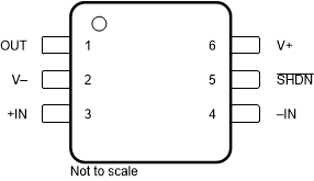
 Figure 4-4 TLV9061S DBV Package,6-Pin SOT-23(Top View)
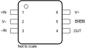
 Figure 4-5 TLV9061S DRY Package,6-Pin USON(Top View)
Table 4-2 Pin Functions: TLV9061S
| PIN | TYPE(1) | DESCRIPTION | ||
|---|---|---|---|---|
| NAME | SOT-23 | USON | ||
| IN– | 4 | 3 | I | Inverting input |
| IN+ | 3 | 1 | I | Noninverting input |
| OUT | 1 | 4 | O | Output |
| SHDN | 5 | 5 | I | Shutdown: low = amp disabled, high = amp enabled. See Shutdown Function section for more information. |
| V– | 2 | 2 | I or — | Negative (low) supply or ground (for single-supply operation) |
| V+ | 6 | 6 | I | Positive (high) supply |
(1) I = input, O = output
 Figure 4-6 TLV9062 D, DGK, PW, or DDF Package,8-Pin SOIC, VSSOP, TSSOP, or SOT-23(Top View)
A. Connect thermal pad to
V–
Figure 4-7 TLV9062 DSG Package,8-Pin WSON With Exposed Thermal Pad(Top View)Table 4-3 Pin Functions: TLV9062
| PIN | TYPE(1) | DESCRIPTION | |
|---|---|---|---|
| NAME | NO. | ||
| IN1– | 2 | I | Inverting input, channel 1 |
| IN1+ | 3 | I | Noninverting input, channel 1 |
| IN2– | 6 | I | Inverting input, channel 2 |
| IN2+ | 5 | I | Noninverting input, channel 2 |
| OUT1 | 1 | O | Output, channel 1 |
| OUT2 | 7 | O | Output, channel 2 |
| V– | 4 | — | Negative (lowest) supply or ground (for single-supply operation) |
| V+ | 8 | — | Positive (highest) supply |
(1) I = input, O = output
 Figure 4-8 TLV9062S DGS Package,10-Pin VSSOP(Top View)
 Figure 4-9 TLV9062S RUG Package,10-Pin X2QFN(Top View)
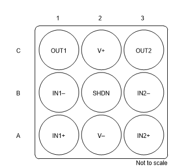
 Figure 4-10 TLV9062S YCK Package
9-Pin DSBGA (WCSP)
Bottom View
Table 4-4 Pin Functions: TLV9062S
| PIN | I/O | DESCRIPTION | |||
|---|---|---|---|---|---|
| NAME | VSSOP | X2QFN | DSBGA (WCSP) | ||
| IN1– | 2 | 9 | B1 | I | Inverting input, channel 1 |
| IN1+ | 3 | 10 | A1 | I | Noninverting input, channel 1 |
| IN2– | 8 | 5 | B3 | I | Inverting input, channel 2 |
| IN2+ | 7 | 4 | A3 | I | Noninverting input, channel 2 |
| OUT1 | 1 | 8 | C1 | O | Output, channel 1 |
| OUT2 | 9 | 6 | C3 | O | Output, channel 2 |
| SHDN1 | 5 | 2 | — | I | Shutdown: low = amp disabled, high = amp enabled, channel 1. See Shutdown Function for more information. |
| SHDN2 | 6 | 3 | — | I | Shutdown: low = amp disabled, high = amp enabled, channel 1. See Shutdown Function for more information. |
| SHDN | — | — | B2 | Shutdown: low = both amplifiers disabled, high = both amplifiers enabled | |
| V– | 4 | 1 | A2 | I or — | Negative (low) supply or ground (for single-supply operation) |
| V+ | 10 | 7 | C2 | I | Positive (high) supply |
 Figure 4-11 TLV9064 RUC Package,14-Pin X2QFN(Top View)
 Figure 4-13 TLV9064 D or PW Package,14-Pin SOIC or TSSOP(Top View)
A. Connect thermal pad to
V–
Figure 4-12 TLV9064 RTE Package,16-Pin WQFN With Exposed Thermal Pad(Top View)Table 4-5 Pin
Functions: TLV9064
| PIN | TYPE(1) | DESCRIPTION | |||
|---|---|---|---|---|---|
| NAME | SOIC, TSSOP |
WQFN | X2QFN | ||
| IN1– | 2 | 16 | 1 | I | Inverting input, channel 1 |
| IN1+ | 3 | 1 | 2 | I | Noninverting input, channel 1 |
| IN2– | 6 | 4 | 5 | I | Inverting input, channel 2 |
| IN2+ | 5 | 3 | 4 | I | Noninverting input, channel 2 |
| IN3– | 9 | 9 | 8 | I | Inverting input, channel 3 |
| IN3+ | 10 | 10 | 9 | I | Noninverting input, channel 3 |
| IN4– | 13 | 13 | 12 | I | Inverting input, channel 4 |
| IN4+ | 12 | 12 | 11 | I | Noninverting input, channel 4 |
| NC | — | 6, 7 | — | — | No internal connection |
| OUT1 | 1 | 15 | 14 | O | Output, channel 1 |
| OUT2 | 7 | 5 | 6 | O | Output, channel 2 |
| OUT3 | 8 | 8 | 7 | O | Output, channel 3 |
| OUT4 | 14 | 14 | 13 | O | Output, channel 4 |
| V– | 11 | 11 | 10 | I or — | Negative (low) supply or ground (for single-supply operation) |
| V+ | 4 | 2 | 3 | I | Positive (high) supply |
(1) I = input, O = output

A. Connect thermal pad to V–
Figure 4-14 TLV9064S RTE Package,16-Pin WQFN With
Exposed Thermal Pad(Top View)Table 4-6 Pin Functions: TLV9064S
| PIN | TYPE(1) | DESCRIPTION | |
|---|---|---|---|
| NAME | NO. | ||
| IN1– | 16 | I | Inverting input, channel 1 |
| IN1+ | 1 | I | Noninverting input, channel 1 |
| IN2– | 4 | I | Inverting input, channel 2 |
| IN2+ | 3 | I | Noninverting input, channel 2 |
| IN3– | 9 | I | Inverting input, channel 3 |
| IN3+ | 10 | I | Noninverting input, channel 3 |
| IN4– | 13 | I | Inverting input, channel 4 |
| IN4+ | 12 | I | Noninverting input, channel 4 |
| OUT1 | 15 | O | Output, channel 1 |
| OUT2 | 5 | O | Output, channel 2 |
| OUT3 | 8 | O | Output, channel 3 |
| OUT4 | 14 | O | Output, channel 4 |
| SHDN12 | 6 | I | Shutdown: low = amp disabled, high = amp enabled. Channel 1. See Shutdown Function section for more information. |
| SHDN34 | 7 | I | Shutdown: low = amp disabled, high = amp enabled. Channel 1. See Shutdown Function section for more information. |
| V– | 11 | I or — | Negative (low) supply or ground (for single-supply operation) |
| V+ | 2 | I | Positive (high) supply |
(1) I = input, O = output