SBOS839M March 2017 – December 2024 TLV9061 , TLV9062 , TLV9064
PRODMIX
- 1
- 1 Features
- 2 Applications
- 3 Description
- Device Comparison Table
- 4 Pin Configuration and Functions
-
5 Specifications
- 5.1 Absolute Maximum Ratings
- 5.2 ESD Ratings
- 5.3 Recommended Operating Conditions
- 5.4 Thermal Information: TLV9061
- 5.5 Thermal Information: TLV9061S
- 5.6 Thermal Information: TLV9062
- 5.7 Thermal Information: TLV9062S
- 5.8 Thermal Information: TLV9064
- 5.9 Thermal Information: TLV9064S
- 5.10 Electrical Characteristics
- 5.11 Typical Characteristics
- 6 Detailed Description
- 7 Application and Implementation
- 8 Device and Documentation Support
- 9 Revision History
- 10Mechanical, Packaging, and Orderable Information
Package Options
Mechanical Data (Package|Pins)
Thermal pad, mechanical data (Package|Pins)
Orderable Information
3 Description
The TLV9061 (single), TLV9062 (dual), and TLV9064 (quad) are single-, dual-, and quad- low-voltage, 1.8V to 5.5V) operational amplifiers, op amps) with rail-to-rail input and output swing capabilities.
These devices are highly cost-effective options for applications where low-voltage operation, a small footprint, and high capacitive load drive are required.
Although the capacitive load drive of the TLV906x is 100pF, the resistive open-loop output impedance makes stabilizing with higher capacitive loads simpler. These op amps are designed specifically for low-voltage operation (1.8V to 5.5V), with performance specifications similar to the OPAx316 and TLVx316 devices.
The TLV906xS devices include a shutdown mode that allow the amplifiers to switch into standby mode with typical current consumption less than 1µA.
The TLV906xS family helps simplify system design, because the family is unity-gain stable, integrates the RFI and EMI rejection filter, and provides no phase reversal in overdrive condition.
Micro size packages, such as X2SON and X2QFN, are offered for all the channel variants (single, dual and quad), along with industry-standard packages, such as SOIC, MSOP, SOT-23, and TSSOP.
| PART NUMBER(3) | PACKAGE(1) | BODY SIZE (NOM)(4) |
|---|---|---|
| TLV9061 | DBV (SOT-23, 5) | 2.90mm × 1.60 mm |
| DCK (SC70, 5) | 2.00mm × 1.25 mm | |
| DRL (SOT-553, 5)(2) | 1.60mm × 1.20 mm | |
| DPW (X2SON, 5) | 0.80mm × 0.80mm | |
| TLV9061S | DBV (SOT-23, 6) | 2.90mm × 1.60 mm |
| DRY (USON, 6) | 1.45mm × 1.00 mm | |
| TLV9062 | D (SOIC, 8) | 4.90mm × 3.90 mm |
| PW (TSSOP, 8) | 3.00mm × 4.40 mm | |
| DGK (VSSOP, 8) | 3.00mm × 3.00 mm | |
| DDF (SOT-23, 8) | 2.90mm × 1.60 mm | |
| DSG (WSON, 8) | 2.00mm × 2.00 mm | |
| TLV9062S | DGS (VSSOP, 10) | 3.00mm × 3.00 mm |
| RUG (X2QFN, 10) | 2.00mm × 1.50mm | |
| YCK (DSBGA, 9) | 1.00mm x 1.00mm | |
| TLV9064 | D (SOIC, 14) | 8.65mm × 3.90 mm |
| PW (TSSOP, 14) | 5.00mm × 4.40 mm | |
| RTE (WQFN, 16) | 3.00mm × 3.00mm | |
| RUC (X2QFN, 14) | 2.00mm × 2.00mm | |
| TLV9064S | RTE (WQFN, 16) | 3.00mm × 3.00mm |
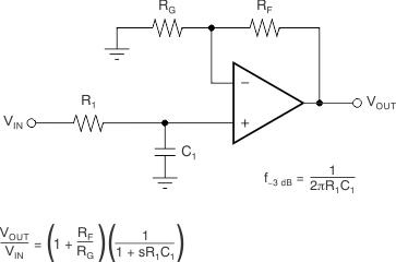
 Single-Pole, Low-Pass
Filter
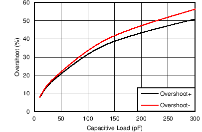
 Small-Signal Overshoot vs
Load Capacitance