SBOSAD6B April   2023  – August 2024 TLV9361-Q1 , TLV9362-Q1 , TLV9364-Q1

PRODUCTION DATA  

  1.   1
  2. Features
  3. Applications
  4. Description
  5. Pin Configuration and Functions
  6. Specifications
    1. 5.1 Absolute Maximum Ratings
    2. 5.2 ESD Ratings
    3. 5.3 Recommended Operating Conditions
    4. 5.4 Thermal Information for Single Channel
    5. 5.5 Thermal Information for Dual Channel
    6. 5.6 Thermal Information for Quad Channel
    7. 5.7 Electrical Characteristics
    8. 5.8 Typical Characteristics
  7. Detailed Description
    1. 6.1 Overview
    2. 6.2 Functional Block Diagram
    3. 6.3 Feature Description
      1. 6.3.1 EMI Rejection
      2. 6.3.2 Thermal Protection
      3. 6.3.3 Capacitive Load and Stability
      4. 6.3.4 Electrical Overstress
      5. 6.3.5 Overload Recovery
      6. 6.3.6 Typical Specifications and Distributions
    4. 6.4 Device Functional Modes
  8. Application and Implementation
    1. 7.1 Application Information
    2. 7.2 Typical Applications
      1. 7.2.1 Low-Side Current Measurement
      2. 7.2.2 Design Requirements
      3. 7.2.3 Detailed Design Procedure
      4. 7.2.4 Application Curves
    3. 7.3 Power Supply Recommendations
    4. 7.4 Layout
      1. 7.4.1 Layout Guidelines
      2. 7.4.2 Layout Example
  9. Device and Documentation Support
    1. 8.1 Device Support
      1. 8.1.1 Development Support
        1. 8.1.1.1 TINA-TI (Free Software Download)
        2. 8.1.1.2 TI Precision Designs
    2. 8.2 Documentation Support
      1. 8.2.1 Related Documentation
    3. 8.3 Receiving Notification of Documentation Updates
    4. 8.4 Support Resources
    5. 8.5 Trademarks
    6. 8.6 Electrostatic Discharge Caution
    7. 8.7 Glossary
  10. Revision History
  11. 10Mechanical, Packaging, and Orderable Information

Package Options

Mechanical Data (Package|Pins)
Thermal pad, mechanical data (Package|Pins)
Orderable Information

Typical Characteristics

at TA = 25°C, VS = ±20V, VCM = VS / 2, RLOAD = 10kΩ (unless otherwise noted)
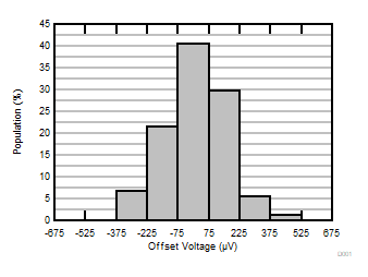
TLV9361-Q1 TLV9362-Q1 TLV9364-Q1 Offset Voltage Production Distribution
Distribution from 74 amplifiers, TA = 25°C
Figure 5-1 Offset Voltage Production Distribution
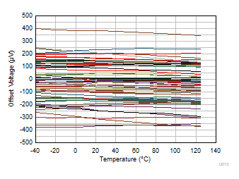
TLV9361-Q1 TLV9362-Q1 TLV9364-Q1 Offset Voltage vs Temperature
VCM = V-
Data from 74 amplifiers
Figure 5-3 Offset Voltage vs Temperature
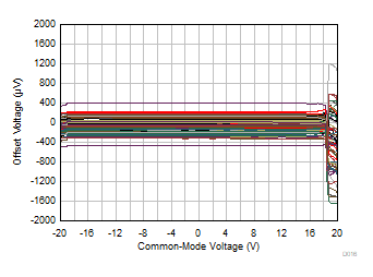
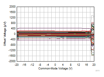
TLV9361-Q1 TLV9362-Q1 TLV9364-Q1 Offset Voltage vs Common-Mode Voltage
TA = 125°C
Data from 74 amplifiers
Figure 5-5 Offset Voltage vs Common-Mode Voltage
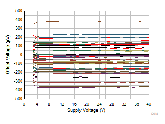
TLV9361-Q1 TLV9362-Q1 TLV9364-Q1 Offset Voltage vs Power Supply
VCM = V–
Data from 74 amplifiers
Figure 5-7 Offset Voltage vs Power Supply
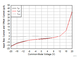
TLV9361-Q1 TLV9362-Q1 TLV9364-Q1 Input
                        Bias Current and Offset Current vs Common-Mode VoltageFigure 5-9 Input Bias Current and Offset Current vs Common-Mode Voltage
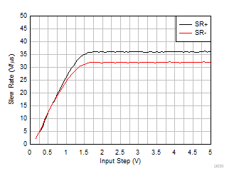
TLV9361-Q1 TLV9362-Q1 TLV9364-Q1 Slew Rate vs Input Step Voltage

G = +1, CL = 20 pF

Figure 5-11 Slew Rate vs Input Step Voltage
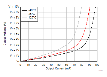
TLV9361-Q1 TLV9362-Q1 TLV9364-Q1 Output Voltage Swing vs Output Current (Sinking)
VS = 40V 
Figure 5-13 Output Voltage Swing vs Output Current (Sinking)
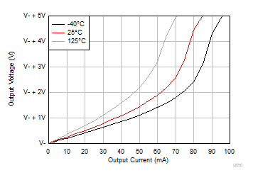
TLV9361-Q1 TLV9362-Q1 TLV9364-Q1 Output Voltage Swing vs Output Current (Sinking)
VS = 5V
Figure 5-15 Output Voltage Swing vs Output Current (Sinking)
TLV9361-Q1 TLV9362-Q1 TLV9364-Q1 CMRR
                        vs Temperature
VS = 40V
Figure 5-17 CMRR vs Temperature
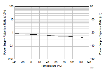
TLV9361-Q1 TLV9362-Q1 TLV9364-Q1 PSRR
                        vs Temperature
Figure 5-19 PSRR vs Temperature
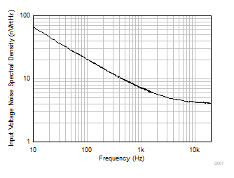
TLV9361-Q1 TLV9362-Q1 TLV9364-Q1 Input
                        Voltage Noise Spectral Density vs FrequencyFigure 5-21 Input Voltage Noise Spectral Density vs Frequency
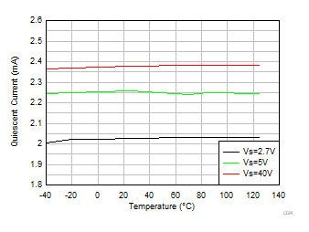
TLV9361-Q1 TLV9362-Q1 TLV9364-Q1 Quiescent Current vs Temperature
VCM = V–
Figure 5-23 Quiescent Current vs Temperature
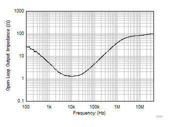
TLV9361-Q1 TLV9362-Q1 TLV9364-Q1 Open-Loop Output Impedance vs FrequencyFigure 5-25 Open-Loop Output Impedance vs Frequency
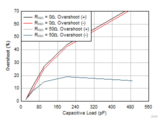
TLV9361-Q1 TLV9362-Q1 TLV9364-Q1 Small-Signal Overshoot vs Capacitive Load
20mVpp Output Step, G = +1
Figure 5-27 Small-Signal Overshoot vs Capacitive Load
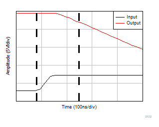
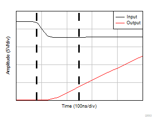
TLV9361-Q1 TLV9362-Q1 TLV9364-Q1 Positive Overload Recovery
G = –10
Figure 5-29 Positive Overload Recovery
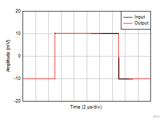
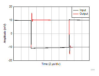
TLV9361-Q1 TLV9362-Q1 TLV9364-Q1 Small-Signal Step Response
CL = 20pF, G = 1, 20mVpp step response
Figure 5-31 Small-Signal Step Response
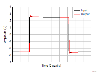
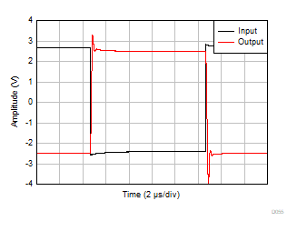
TLV9361-Q1 TLV9362-Q1 TLV9364-Q1 Large-Signal Step Response
CL = 20pF, G = 1, 5Vpp step response
Figure 5-33 Large-Signal Step Response
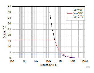
TLV9361-Q1 TLV9362-Q1 TLV9364-Q1 Maximum Output Voltage vs FrequencyFigure 5-35 Maximum Output Voltage vs Frequency
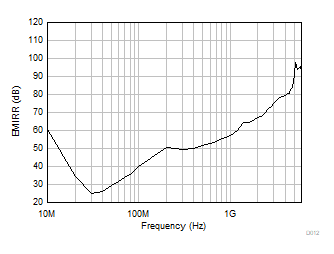
TLV9361-Q1 TLV9362-Q1 TLV9364-Q1 EMIRR
                        (Electromagnetic Interference Rejection Ratio) vs FrequencyFigure 5-37 EMIRR (Electromagnetic Interference Rejection Ratio) vs Frequency
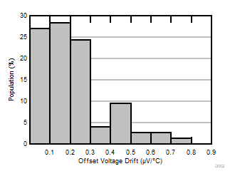
TLV9361-Q1 TLV9362-Q1 TLV9364-Q1 Offset Voltage Drift Distribution
Distribution from 74 amplifiers
Figure 5-2 Offset Voltage Drift Distribution
TLV9361-Q1 TLV9362-Q1 TLV9364-Q1 Offset Voltage vs Common-Mode Voltage
TA = 25°C
Data from 74 amplifiers
Figure 5-4 Offset Voltage vs Common-Mode Voltage
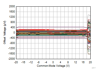
TLV9361-Q1 TLV9362-Q1 TLV9364-Q1 Offset Voltage vs Common-Mode Voltage
TA = –40°C
Data from 74 amplifiers
Figure 5-6 Offset Voltage vs Common-Mode Voltage
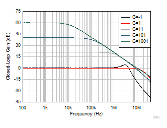
TLV9361-Q1 TLV9362-Q1 TLV9364-Q1 Closed-Loop Gain vs FrequencyFigure 5-8 Closed-Loop Gain vs Frequency
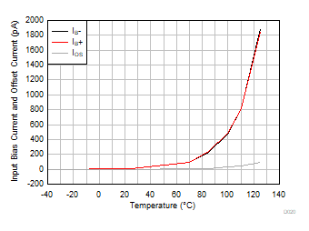
TLV9361-Q1 TLV9362-Q1 TLV9364-Q1 Input
                        Bias Current and Offset Current vs TemperatureFigure 5-10 Input Bias Current and Offset Current vs Temperature
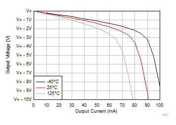
TLV9361-Q1 TLV9362-Q1 TLV9364-Q1 Output Voltage Swing vs Output Current (Sourcing)
VS = 40 V
Figure 5-12 Output Voltage Swing vs Output Current (Sourcing)
TLV9361-Q1 TLV9362-Q1 TLV9364-Q1 Output Voltage Swing vs Output Current (Sourcing)
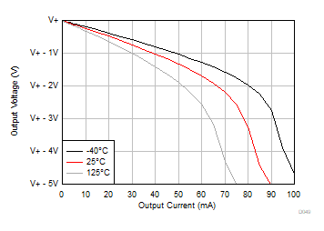
VS = 5V
Figure 5-14 Output Voltage Swing vs Output Current (Sourcing)
TLV9361-Q1 TLV9362-Q1 TLV9364-Q1 CMRR
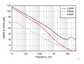
                        and PSRR vs Frequency
 
Figure 5-16 CMRR and PSRR vs Frequency
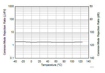
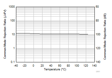
TLV9361-Q1 TLV9362-Q1 TLV9364-Q1 CMRR
                        vs Temperature
VS = 5V
Figure 5-18 CMRR vs Temperature
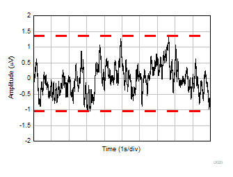
TLV9361-Q1 TLV9362-Q1 TLV9364-Q1 0.1Hz to 10-Hz
            NoiseFigure 5-20 0.1Hz to 10-Hz Noise
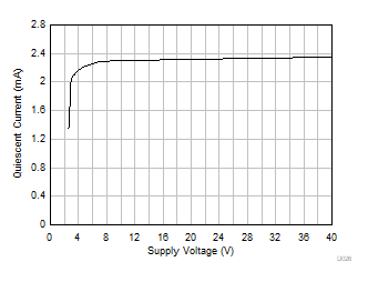
TLV9361-Q1 TLV9362-Q1 TLV9364-Q1 Quiescent Current vs Supply Voltage
VCM = V–
Figure 5-22 Quiescent Current vs Supply Voltage
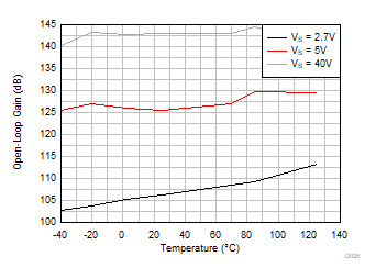
TLV9361-Q1 TLV9362-Q1 TLV9364-Q1 Open-Loop Voltage Gain vs Temperature (dB)Figure 5-24 Open-Loop Voltage Gain vs Temperature (dB)
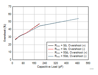
TLV9361-Q1 TLV9362-Q1 TLV9364-Q1 Small-Signal Overshoot vs Capacitive Load
20mVpp Output Step, G = -1
Figure 5-26 Small-Signal Overshoot vs Capacitive Load
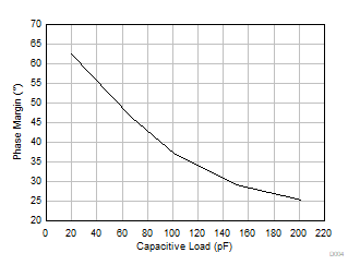
TLV9361-Q1 TLV9362-Q1 TLV9364-Q1 Phase
                        Margin vs Capacitive Load
G = +1
Figure 5-28 Phase Margin vs Capacitive Load
TLV9361-Q1 TLV9362-Q1 TLV9364-Q1 Negative Overload Recovery
G = –10
Figure 5-30 Negative Overload Recovery
TLV9361-Q1 TLV9362-Q1 TLV9364-Q1 Small-Signal Step Response
CL = 20pF, G = -1, 20mVpp step response
Figure 5-32 Small-Signal Step Response
TLV9361-Q1 TLV9362-Q1 TLV9364-Q1 Large-Signal Step Response
CL = 20pF, G = -1, 5Vpp step response
Figure 5-34 Large-Signal Step Response
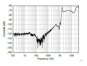
TLV9361-Q1 TLV9362-Q1 TLV9364-Q1 Channel Separation vs FrequencyFigure 5-36 Channel Separation vs Frequency