SBASAJ1B December   2022  – August 2024 TMAG5115

PRODUCTION DATA  

  1.   1
  2. Features
  3. Applications
  4. Description
  5. Device Comparison
  6. Pin Configuration and Functions
  7. Specifications
    1. 6.1 Absolute Maximum Ratings
    2. 6.2 ESD Ratings
    3. 6.3 Recommended Operating Conditions
    4. 6.4 Thermal Information
    5. 6.5 Electrical Characteristics
    6. 6.6 Magnetic Characteristics
    7. 6.7 Typical Characteristics
  8. Detailed Description
    1. 7.1 Overview
    2. 7.2 Functional Block Diagram
    3. 7.3 Feature Description
      1. 7.3.1 Field Direction Definition
      2. 7.3.2 Device Output
      3. 7.3.3 Power-On Time
      4. 7.3.4 Output Stage
      5. 7.3.5 Protection Circuits
        1. 7.3.5.1 Short-Circuit Protection
        2. 7.3.5.2 Overtemperature Protection
    4. 7.4 Device Functional Modes
  9. Application and Implementation
    1. 8.1 Application Information
    2. 8.2 Typical Applications
      1. 8.2.1 Standard Circuit
        1. 8.2.1.1 Design Requirements
        2. 8.2.1.2 Detailed Design Procedure
          1. 8.2.1.2.1 Configuration Example
        3. 8.2.1.3 Application Curves
    3. 8.3 Power Supply Recommendations
    4. 8.4 Layout
      1. 8.4.1 Layout Guidelines
      2. 8.4.2 Layout Example
  10. Device and Documentation Support
    1. 9.1 Device Support
      1. 9.1.1 Hall Sensor Location
    2. 9.2 Receiving Notification of Documentation Updates
    3. 9.3 Support Resources
    4. 9.4 Trademarks
    5. 9.5 Electrostatic Discharge Caution
    6. 9.6 Glossary
  11. 10Revision History
  12. 11Mechanical, Packaging, and Orderable Information

Package Options

Mechanical Data (Package|Pins)
Thermal pad, mechanical data (Package|Pins)
Orderable Information

Output Stage

Figure 7-7 shows the TMAG5115 open-drain NMOS output structure, rated to sink up to 15 mA of current.

Note:

Vref is not restricted to VCC. The allowable voltage range of this pin is specified in the Recommended Operating Conditions.

TMAG5115 NMOS Open-Drain Output Figure 7-7 NMOS Open-Drain Output

Select a value for C2 based on the system bandwidth specifications as shown in Equation 1.

Equation 1. TMAG5115

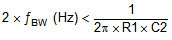
Most applications do not require this C2 filtering capacitor.