SBOSA36A January 2021 – July 2021 TMCS1108
PRODUCTION DATA
- 1 Features
- 2 Applications
- 3 Description
- 4 Revision History
- 5 Device Comparison
- 6 Pin Configuration and Functions
- 7 Specifications
- 8 Parameter Measurement Information
- 9 Detailed Description
- 10Application and Implementation
- 11Power Supply Recommendations
- 12Layout
- 13Device and Documentation Support
- 14Mechanical, Packaging, and Orderable Information
Package Options
Refer to the PDF data sheet for device specific package drawings
Mechanical Data (Package|Pins)
- D|8
Thermal pad, mechanical data (Package|Pins)
Orderable Information
9.3.2.3 Transient Response
The TMCS1108 signal chain includes a precision analog front end followed by a sampled integrator. At the end of each integration cycle, the signal propagates to the output. Depending on the alignment of a change in input current relative to the sampling window, the output might not settle to the final signal until the second integration cycle. Figure 9-6 shows a typical output waveform response to a 10-kHz sine wave input current. For a slowly varying input current signal, the output is a discrete time representation with a phase delay of the integration sampling window. Adding a first order filter of 100 kHz effectively smooths the output waveform with minimal impact to phase response.
 Figure 9-6 Response Behavior to 10-kHz Sine Wave Input
Current
Figure 9-6 Response Behavior to 10-kHz Sine Wave Input
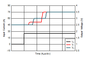
CurrentFigure 9-7 shows two transient waveforms to an input-current step event, but occurring at different times during the sampling interval. In both cases, the full transition of the output takes two sampling intervals to reach the final output value. The timing of the current event relative to the sampling window determines the proportional amplitude of the first and second sampling intervals.
 Figure 9-7 Transient Response to Input-Current Step Sufficient for 1-V Output Swing
The output value is effectively an average over the sampling window; therefore, a large-enough current transient can drive the output voltage to near the full scale range in the first sample response. This condition is likely to be true in the case of a short-circuit or fault event. Figure 9-8 shows an input-current step twice the full scale measurable range with two output voltage responses illustrating the effect of the sampling window. The relative timing and size of the input current transition determines both the time and amplitude of the first output transition. In either case, the total response time is slightly longer than one integration period.
 Figure 9-8 Transient Response to a Large Input Current Step