SBOSA36A January 2021 – July 2021 TMCS1108
PRODUCTION DATA
- 1 Features
- 2 Applications
- 3 Description
- 4 Revision History
- 5 Device Comparison
- 6 Pin Configuration and Functions
- 7 Specifications
- 8 Parameter Measurement Information
- 9 Detailed Description
- 10Application and Implementation
- 11Power Supply Recommendations
- 12Layout
- 13Device and Documentation Support
- 14Mechanical, Packaging, and Orderable Information
Package Options
Refer to the PDF data sheet for device specific package drawings
Mechanical Data (Package|Pins)
- D|8
Thermal pad, mechanical data (Package|Pins)
Orderable Information
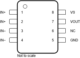
6 Pin Configuration and Functions
 Figure 6-1 D
Package8-Pin SOICTop View
Figure 6-1 D
Package8-Pin SOICTop ViewTable 6-1 Pin Functions
| PIN | I/O | DESCRIPTION | |
|---|---|---|---|
| NO. | NAME | ||
| 1 | IN+ | Analog input | Input current positive pin |
| 2 | IN+ | Analog input | Input current positive pin |
| 3 | IN– | Analog input | Input current negative pin |
| 4 | IN– | Analog input | Input current negative pin |
| 5 | GND | Analog | Ground |
| 6 | NC | No Connect | No connect. Pin can tolerate a capacitive or resistive connection to GND or VS (recommend short to GND if acceptable). |
| 7 | VOUT | Analog output | Output voltage |
| 8 | VS | Analog | Power supply |