SBOS581B September 2011 – June 2022 TMP100-Q1 , TMP101-Q1
PRODUCTION DATA
- 1 Features
- 2 Applications
- 3 Description
- 4 Revision History
- 5 Pin Configuration and Functions
- 6 Specifications
-
7 Detailed Description
- 7.1 Overview
- 7.2 Functional Block Diagram
- 7.3
Feature Description
- 7.3.1 Digital Temperature Output
- 7.3.2 Serial Interface
- 7.3.3 Bus Overview
- 7.3.4 Serial Bus Address
- 7.3.5 Writing and Reading to the TMP100-Q1 and TMP101-Q1
- 7.3.6 Target Mode Operations
- 7.3.7 SMBus Alert Function
- 7.3.8 General Call
- 7.3.9 High-Speed Mode
- 7.3.10 POR (Power-On Reset)
- 7.3.11 Timing Diagrams
- 7.4 Device Functional Modes
- 7.5 Programming
- 8 Application and Implementation
- 9 Power Supply Recommendations
- 10Layout
- 11Device and Documentation Support
- 12Mechanical, Packaging, and Orderable Information
Package Options
Mechanical Data (Package|Pins)
- DBV|6
Thermal pad, mechanical data (Package|Pins)
Orderable Information
7.3.11 Timing Diagrams
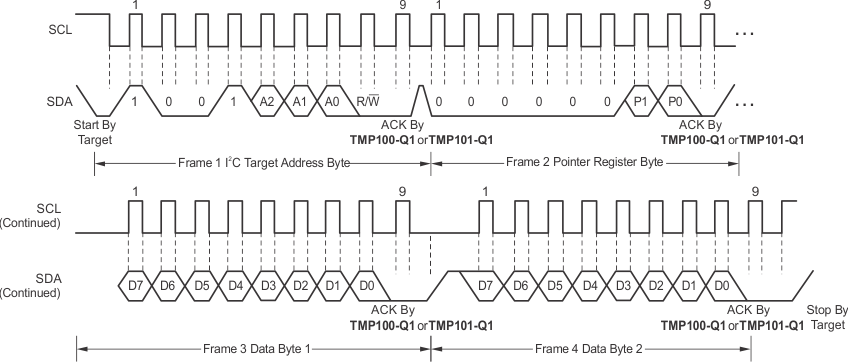
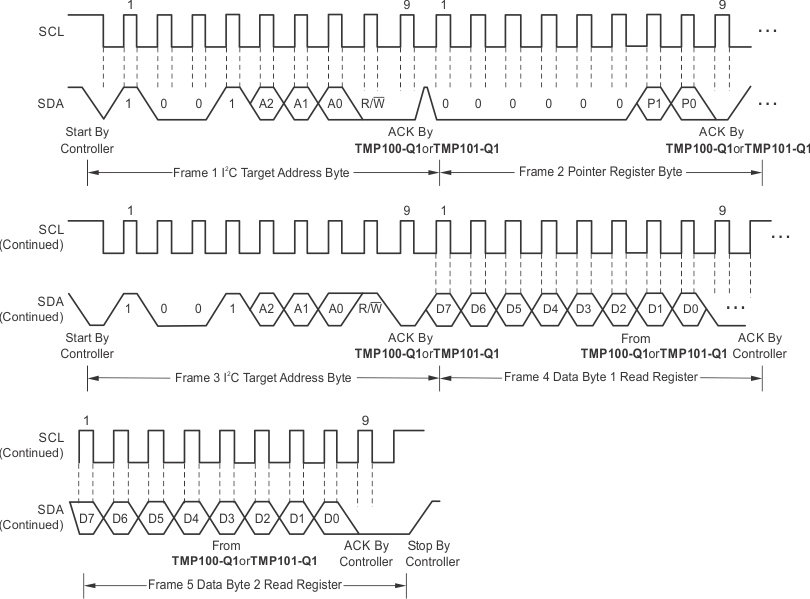
The TMP100-Q1 and TMP101-Q1 devices are Two-Wire, SMBUs, and I2C interface-compatible. Figure 7-3 to Figure 7-6 describe the various operations on the TMP100-Q1 and TMP101-Q1. The following list provides bus definitions. Parameters for Figure 7-3 are defined in the Section 6.6 table.
Bus Idle: Both SDA and SCL lines remain HIGH.
Start Data Transfer: A change in the state of the SDA line, from HIGH to LOW, while the SCL line is HIGH, defines a START condition. Each data transfer is initiated with a START condition.
Stop Data Transfer: A change in the state of the SDA line from LOW to HIGH while the SCL line is HIGH defines a STOP condition. Each data transfer is terminated with a repeated START or STOP condition.
Data Transfer: The number of data bytes transferred between a START and a STOP condition is not limited and is determined by the controller device. The receiver acknowledges the transfer of data.
Acknowledge: Each receiving device, when addressed, is obliged to generate an Acknowledge bit. A device that acknowledges must pull down the SDA line during the Acknowledge clock pulse in such a way that the SDA line is stable LOW during the HIGH period of the Acknowledge clock pulse. Setup and hold times must be taken into account. On a controller receive, the termination of the data transfer can be signaled by the controller generating a Not-Acknowledge on the last byte that is transmitted by the target.
 Figure 7-3 I2C Timing Diagram
 Figure 7-4 I2C Timing Diagram for Write Word Format
 Figure 7-5 I2C Timing Diagram for Read Word Format
 Figure 7-6 Timing Diagram for SMBus ALERT