SBOS581B September   2011  – June 2022 TMP100-Q1 , TMP101-Q1

PRODUCTION DATA  

  1. Features
  2. Applications
  3. Description
  4. Revision History
  5. Pin Configuration and Functions
  6. Specifications
    1. 6.1 Absolute Maximum Ratings
    2. 6.2 ESD Ratings
    3. 6.3 Recommended Operating Conditions
    4. 6.4 Thermal Information
    5. 6.5 Electrical Characteristics
    6. 6.6 Timing Requirements
    7. 6.7 Typical Characteristics
  7. Detailed Description
    1. 7.1 Overview
    2. 7.2 Functional Block Diagram
    3. 7.3 Feature Description
      1. 7.3.1  Digital Temperature Output
      2. 7.3.2  Serial Interface
      3. 7.3.3  Bus Overview
      4. 7.3.4  Serial Bus Address
      5. 7.3.5  Writing and Reading to the TMP100-Q1 and TMP101-Q1
      6. 7.3.6  Target Mode Operations
        1. 7.3.6.1 Target Receiver Mode
        2. 7.3.6.2 Target Transmitter Mode
      7. 7.3.7  SMBus Alert Function
      8. 7.3.8  General Call
      9. 7.3.9  High-Speed Mode
      10. 7.3.10 POR (Power-On Reset)
      11. 7.3.11 Timing Diagrams
    4. 7.4 Device Functional Modes
      1. 7.4.1 Shutdown Mode (SD)
      2. 7.4.2 OS/ALERT (OS)
      3. 7.4.3 Thermostat Mode (TM)
      4. 7.4.4 Comparator Mode (TM = 0)
      5. 7.4.5 Interrupt Mode (TM = 1)
    5. 7.5 Programming
      1. 7.5.1 Pointer Register
        1. 7.5.1.1 Pointer Register Byte (pointer = N/A) [reset = 00h]
        2. 7.5.1.2 Pointer Addresses of the TMP100-Q1 and TMP101-Q1 Registers
      2. 7.5.2 Temperature Register
      3. 7.5.3 Configuration Register
        1. 7.5.3.1 Shutdown Mode (SD)
        2. 7.5.3.2 Thermostat Mode (TM)
        3. 7.5.3.3 Polarity (POL)
        4. 7.5.3.4 Fault Queue (F1, F0)
        5. 7.5.3.5 Converter Resolution (R1, R0)
        6. 7.5.3.6 OS/ALERT (OS)
      4. 7.5.4 High- and Low-Limit Registers
  8. Application and Implementation
    1. 8.1 Application Information
    2. 8.2 Typical Application
      1. 8.2.1 Design Requirements
      2. 8.2.2 Detailed Design Procedure
      3. 8.2.3 Application Curve
  9. Power Supply Recommendations
  10. 10Layout
    1. 10.1 Layout Guidelines
    2. 10.2 Layout Examples
  11. 11Device and Documentation Support
    1. 11.1 Receiving Notification of Documentation Updates
    2. 11.2 Support Resources
    3. 11.3 Trademarks
    4. 11.4 Electrostatic Discharge Caution
    5. 11.5 Glossary
  12. 12Mechanical, Packaging, and Orderable Information

Package Options

Mechanical Data (Package|Pins)
Thermal pad, mechanical data (Package|Pins)
Orderable Information

Application Curve

Figure 8-3 shows the step response of the TMP100-Q1 and TMP101-Q1 devices to a submersion in an oil bath of 100°C from room temperature (27°C). The time constant, or the time for the output to reach 63% of the input step, is 0.9 s. The time-constant result depends on the PCB that the TMP100-Q1 and TMP101-Q1 devices are mounted. For this test, the TMP100-Q1 and TMP101-Q1 devices are soldered to a two-layer PCB that measures 0.375 inch × 0.437 inch.
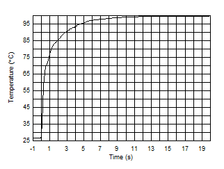
GUID-E574BAD2-D81B-48A3-8272-19C575097D32-low.gifFigure 8-3 Temperature Step Response