SBOS854F March 2018 – June 2024 TMP1075
PRODUCTION DATA
- 1
- 1 Features
- 2 Applications
- 3 Description
- 4 Device Comparison
- 5 Pin Configuration and Functions
-
6 Specifications
- 6.1 Absolute Maximum Ratings
- 6.2 ESD Ratings
- 6.3 Recommended Operating Conditions
- 6.4 Thermal Information
- 6.5 Electrical Characteristics:TMP1075
- 6.6 Electrical Characteristics: TMP1075N
- 6.7 Timing Requirements:TMP1075
- 6.8 Timing Requirements: TMP1075N
- 6.9 Switching Characteristics
- 6.10 Timing Diagrams
- 6.11 Typical Characteristics
-
7 Detailed Description
- 7.1 Overview
- 7.2 Functional Block Diagram
- 7.3
Feature Description
- 7.3.1 Digital Temperature Output
- 7.3.2
I2C and SMBus Serial Interface
- 7.3.2.1 Bus Overview
- 7.3.2.2 Serial Bus Address
- 7.3.2.3 Pointer Register
- 7.3.2.4 Writing and Reading to the TMP1075
- 7.3.2.5 Operation Mode
- 7.3.2.6 SMBus Alert Function
- 7.3.2.7 General Call- Reset Function
- 7.3.2.8 High-Speed Mode (HS)
- 7.3.2.9 Coexists in I3C Mixed Fast Mode
- 7.3.2.10 Time-Out Function
- 7.3.3 Timing Diagrams
- 7.3.4 Two-Wire Timing Diagrams
- 7.4 Device Functional Modes
- 7.5
Register Map
- 7.5.1
Register Descriptions
- 7.5.1.1 Temperature Register (address = 00h) [default reset = 0000h]
- 7.5.1.2 Configuration Register (address = 01h) [default reset = 00FFh (60A0h TMP1075N)]
- 7.5.1.3 Low Limit Register (address = 02h) [default reset = 4B00h]
- 7.5.1.4 High Limit Register (address = 03h) [default reset = 5000h]
- 7.5.1.5 Device ID Register (address = 0Fh) [default reset = 7500]
- 7.5.1
Register Descriptions
- 8 Application and Implementation
- 9 Device and Documentation Support
- 10Revision History
- 11Mechanical, Packaging, and Orderable Information
Package Options
Mechanical Data (Package|Pins)
Thermal pad, mechanical data (Package|Pins)
- DSG|8
Orderable Information
7.4.4.3 Polarity Mode (POL)
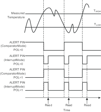
The polarity bit allows the user to adjust the polarity of the ALERT pin output. If the POL bit is set to 0 (default), the ALERT pin becomes active low. When POL bit is set to 1, the ALERT pin becomes active high and the state of the ALERT pin is inverted. Figure 7-10 shows the operation of the ALERT pin in various modes.
 Figure 7-10 Output Transfer Function Diagrams