SNIS233A February   2024  – July 2024 TMP110

PRODUCTION DATA  

  1.   1
  2. Features
  3. Applications
  4. Description
  5. Related Products
  6. Pin Configuration and Functions
  7. Specifications
    1. 6.1 Absolute Maximum Ratings
    2. 6.2 ESD Ratings
    3. 6.3 Recommended Operating Conditions
    4. 6.4 Thermal Information
    5. 6.5 Electrical Characteristics
    6. 6.6 I2C Interface Timing
    7. 6.7 Timing Diagrams
    8. 6.8 Typical Characteristics
  8. Detailed Description
    1. 7.1 Overview
    2. 7.2 Functional Block Diagram
    3. 7.3 Feature Description
      1. 7.3.1 Digital Temperature Output
      2. 7.3.2 Decoding Temperature Data
      3. 7.3.3 Temperature Limits and Alert
    4. 7.4 Device Functional Modes
      1. 7.4.1 Continuous-Conversion Mode
      2. 7.4.2 One-Shot Mode
    5. 7.5 Programming
      1. 7.5.1 Serial Interface
      2. 7.5.2 Bus Overview
      3. 7.5.3 Device Address
      4. 7.5.4 Bus Transactions
        1. 7.5.4.1 Writes
        2. 7.5.4.2 Reads
        3. 7.5.4.3 General Call Reset Function
        4. 7.5.4.4 SMBus Alert Response
        5. 7.5.4.5 Time-Out Function
        6. 7.5.4.6 Coexist on I3C Mixed Bus
  9. Register Map
    1. 8.1 Temp_Result Register (address = 00h) [reset = xxxxh]
    2. 8.2 Configuration Register (address = 01h) [reset = 60A0h]
    3. 8.3 TLow_Limit Register (address = 02h) [reset = 4B00h]
    4. 8.4 THigh_Limit Register (address = 03h) [reset = 5000h]
  10. Application and Implementation
    1. 9.1 Application Information
    2. 9.2 Equal I2C Pullup and Supply Application
      1. 9.2.1 Design Requirements
      2. 9.2.2 Detailed Design Procedure
      3. 9.2.3 Application Curve
      4. 9.2.4 Power Supply Recommendations
    3. 9.3 Layout
      1. 9.3.1 Layout Guidelines
      2. 9.3.2 Layout Example
  11. 10Device and Documentation Support
    1. 10.1 Documentation Support
      1. 10.1.1 Related Documentation
    2. 10.2 Receiving Notification of Documentation Updates
    3. 10.3 Support Resources
    4. 10.4 Trademarks
    5. 10.5 Electrostatic Discharge Caution
    6. 10.6 Glossary
  12. 11Revision History
  13. 12Mechanical, Packaging, and Orderable Information

Package Options

Mechanical Data (Package|Pins)
Thermal pad, mechanical data (Package|Pins)
Orderable Information

Bus Overview

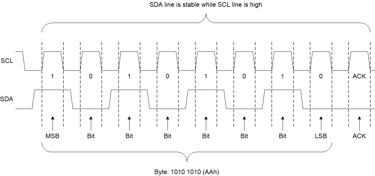
The physical I2C interface consists of the serial clock (SCL) and serial data (SDA) lines. The SDA line must be connected to a supply through a pullup resistor. The size of the pullup resistor is determined by the amount of capacitance on the I2C lines, the communication frequency and I2C bus voltage. For further details, see the I2C Pullup Resistor Calculation application note. Data transfer can be initiated only when the bus is idle. A bus is considered idle if both SDA and SCL lines are high after a STOP condition or time out events (see Figure 7-7 and Figure 7-8).
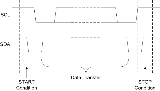
TMP110 Definition of Start and Stop ConditionsFigure 7-7 Definition of Start and Stop Conditions
TMP110 Bit TransferFigure 7-8 Bit Transfer