SNIS217C december 2020 – may 2023 TMP139
PRODUCTION DATA
- 1 Features
- 2 Applications
- 3 Description
- 4 Revision History
- 5 Pin Configuration and Functions
- 6 Specifications
-
7 Detailed Description
- 7.1 Overview
- 7.2 Functional Block Diagram
- 7.3 Feature Description
- 7.4 Device Functional Modes
- 7.5 Programming
- 7.6 Register Map
- 8 Application and Implementation
- 9 Device and Documentation Support
- 10Mechanical, Packaging, and Orderable Information
Package Options
Refer to the PDF data sheet for device specific package drawings
Mechanical Data (Package|Pins)
- YAH|6
Thermal pad, mechanical data (Package|Pins)
Orderable Information
7.4.3.3 Host I2C Read Operation in Default Read Address Pointer Mode
The TMP139 provides a default read address pointer mode as shown in Figure 7-8 to read a specific register on the I2C bus. Since the number of bytes to be sent by the host are two less than a standard I2C read operation, this mode provides for a more efficient polling mechanism. The MR18 register, bit DEF_RD_ADDR_POINT_EN is used to enable the mode and bits DEF_RD_ADDR_POINT_Start are used to set the default read address pointer to a specific register in the register map. When enabled, the TMP139 shall set the internal read address pointer to the specific register when there is a Stop condition on the bus.
 Figure 7-8 I2C Default Read Address Pointer Mode
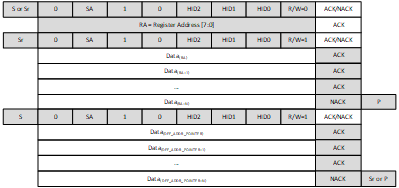
There can be two specific cases in this mode of operation. In the first case as shown in Figure 7-9, there is a normal I2C read preceding the default read mode. If a Stop precedes the Start, then the internal read address pointer shall be set to the default address pointer and subsequent data reads shall result in the data bytes sent by the TMP139 corresponding to the default read address pointer. If a Repeated Start is issued instead of a Stop, then the TMP139 shall send data based on the default read address pointer.
 Figure 7-9 I2C normal read followed by a Default Read Address
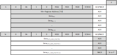
In the second case as shown in Figure 7-10, there is a normal I2C write preceding the default read mode. If there is a Stop, followed by a write bus operation and then a Repeated Start for the read mode, then the TMP139 shall update its internal read address pointer to the default read address and transmit bytes to the host.
 Figure 7-10 I2C normal write followed by a Default Read Address