SNIS217C december 2020 – may 2023 TMP139
PRODUCTION DATA
- 1 Features
- 2 Applications
- 3 Description
- 4 Revision History
- 5 Pin Configuration and Functions
- 6 Specifications
-
7 Detailed Description
- 7.1 Overview
- 7.2 Functional Block Diagram
- 7.3 Feature Description
- 7.4 Device Functional Modes
- 7.5 Programming
- 7.6 Register Map
- 8 Application and Implementation
- 9 Device and Documentation Support
- 10Mechanical, Packaging, and Orderable Information
Package Options
Refer to the PDF data sheet for device specific package drawings
Mechanical Data (Package|Pins)
- YAH|6
Thermal pad, mechanical data (Package|Pins)
Orderable Information
5 Pin Configuration and Functions
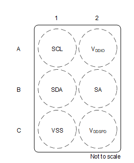
 Figure 5-1 YAH
Package6-Pin DSBGATop View
Figure 5-1 YAH
Package6-Pin DSBGATop ViewTable 5-1 Pin Functions
| PIN | I/O | DESCRIPTION | |
|---|---|---|---|
| NAME | BALL | ||
| SA | B2 | I | Address select. Connected to VDDSPD or GND |
| SCL | A1 | I | Serial clock |
| SDA | B1 | I/O | Serial data input and output. Pin may be open drain or push-pull in I3C mode and open drain in I2C mode |
| VDDIO | A2 | I | Supply voltage for sensor I/Os |
| VDDSPD | C2 | I | Supply voltage for sensor core |
| VSS | C1 | — | Ground |