SBOSA45D February 2022 – January 2025 TMP1826
PRODUCTION DATA
- 1
- 1 Features
- 2 Applications
- 3 Description
- 4 Description (cont.)
- 5 Device Comparison
- 6 Pin Configuration and Functions
- 7 Specifications
-
8 Detailed Description
- 8.1 Overview
- 8.2 Functional Block Diagram
- 8.3
Feature Description
- 8.3.1 Power Up
- 8.3.2 Power Mode Switch
- 8.3.3 Bus Pullup Resistor
- 8.3.4 Temperature Results
- 8.3.5 Temperature Offset
- 8.3.6 Temperature Alert
- 8.3.7 Standard Device Address
- 8.3.8 Flexible Device Address
- 8.3.9 CRC Generation
- 8.3.10 Functional Register Map
- 8.3.11 User Memory Map
- 8.3.12 Bit Communication
- 8.3.13 Bus Speed
- 8.3.14 NIST Traceability
- 8.4
Device Functional Modes
- 8.4.1 Conversion Modes
- 8.4.2 Alert Function
- 8.4.3
1-Wire® Interface Communication
- 8.4.3.1 Bus Reset Phase
- 8.4.3.2 Address Phase
- 8.4.3.3
Function Phase
- 8.4.3.3.1 CONVERTTEMP (44h)
- 8.4.3.3.2 WRITE SCRATCHPAD-1 (4Eh)
- 8.4.3.3.3 READ SCRATCHPAD-1 (BEh)
- 8.4.3.3.4 COPY SCRATCHPAD-1 (48h)
- 8.4.3.3.5 WRITE SCRATCHPAD-2 (0Fh)
- 8.4.3.3.6 READ SCRATCHPAD-2 (AAh)
- 8.4.3.3.7 COPY SCRATCHPAD-2 (55h)
- 8.4.3.3.8 READ EEPROM (F0h)
- 8.4.3.3.9 GPIO WRITE (A5h)
- 8.4.3.3.10 GPIO READ (F5h)
- 8.4.4 NVM Operations
- 8.5
Programming
- 8.5.1 Single Device Temperature Conversion and Read
- 8.5.2 Multiple Device Temperature Conversion and Read
- 8.5.3 Register Scratchpad-1 Update and Commit
- 8.5.4 Single Device EEPROM Programming and Verify
- 8.5.5 Single Device EEPROM Page Lock Operation
- 8.5.6 Multiple Device IO Read
- 8.5.7 Multiple Device IO Write
- 8.6
Register Map
- 8.6.1 Temperature Result LSB Register (Scratchpad-1 offset = 00h) [reset = 00h]
- 8.6.2 Temperature Result MSB Register (Scratchpad-1 offset = 01h) [reset = 00h]
- 8.6.3 Status Register (Scratchpad-1 offset = 02h) [reset = 3Ch]
- 8.6.4 Device Configuration-1 Register (Scratchpad-1 offset = 04h) [reset = 70h]
- 8.6.5 Device Configuration-2 Register (Scratchpad-1 offset = 05h) [reset = 80h]
- 8.6.6 Short Address Register (Scratchpad-1 offset = 06h) [reset = 00h]
- 8.6.7 Temperature Alert Low LSB Register (Scratchpad-1 offset = 08h) [reset = 00h]
- 8.6.8 Temperature Alert Low MSB Register (Scratchpad-1 offset = 09h) [reset = 00h]
- 8.6.9 Temperature Alert High LSB Register (Scratchpad-1 offset = 0Ah) [reset = F0h]
- 8.6.10 Temperature Alert High MSB Register (Scratchpad-1 offset = 0Bh) [reset = 07h]
- 8.6.11 Temperature Offset LSB Register (Scratchpad-1 offset = 0Ch) [reset = 00h]
- 8.6.12 Temperature Offset MSB Register (Scratchpad-1 offset = 0Dh) [reset = 00h]
- 8.6.13 IO Read Register [reset = F0h]
- 8.6.14 IO Configuration Register [reset = 00h]
- 9 Application and Implementation
- 10Device and Documentation Support
- 11Revision History
- 12Mechanical, Packaging, and Orderable Information
Package Options
Mechanical Data (Package|Pins)
Thermal pad, mechanical data (Package|Pins)
- NGR|8
Orderable Information
7.8 Timing Diagrams
 Figure 7-1 Bus Reset Timing
Diagram
 Figure 7-2 Write Timing Diagram
 Figure 7-3 Read Timing Diagram
 Figure 7-4 VDD Powered
Initialization Timing Diagram
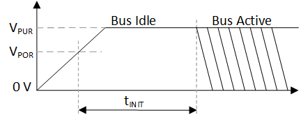
 Figure 7-5 Bus Powered Initialization
Timing Diagram
 Figure 7-6 Glitch Filter Timing
Diagram