SBOSA15A september 2022 – may 2023 TMP1827
PRODUCTION DATA
- 1
- 1 Features
- 2 Applications
- 3 Description
- 4 Revision History
- 5 Description (cont.)
- 6 Device Comparison
- 7 Pin Configuration and Functions
- 8 Specifications
-
9 Detailed Description
- 9.1 Overview
- 9.2 Functional Block Diagram
- 9.3
Feature Description
- 9.3.1 Power Up
- 9.3.2 Power Mode Switch
- 9.3.3 Bus Pullup Resistor
- 9.3.4 Temperature Results
- 9.3.5 Temperature Offset
- 9.3.6 Temperature Alert
- 9.3.7 Standard Device Address
- 9.3.8 Flexible Device Address
- 9.3.9 CRC Generation
- 9.3.10 Functional Register Map
- 9.3.11 User Memory Map
- 9.3.12 SHA-256-HMAC Authentication Block
- 9.3.13 Bit Communication
- 9.3.14 Bus Speed
- 9.3.15 NIST Traceability
- 9.4
Device Functional Modes
- 9.4.1 Conversion Modes
- 9.4.2 Alert Function
- 9.4.3
1-Wire Interface Communication
- 9.4.3.1 Bus Reset Phase
- 9.4.3.2 Address Phase
- 9.4.3.3
Function Phase
- 9.4.3.3.1 CONVERTTEMP (44h)
- 9.4.3.3.2 WRITE SCRATCHPAD-1 (4Eh)
- 9.4.3.3.3 READ SCRATCHPAD-1 (BEh)
- 9.4.3.3.4 COPY SCRATCHPAD-1 (48h)
- 9.4.3.3.5 WRITE SCRATCHPAD-2 (0Fh)
- 9.4.3.3.6 READ SCRATCHPAD-2 (AAh)
- 9.4.3.3.7 COPY SCRATCHPAD-2 (55h)
- 9.4.3.3.8 READ EEPROM (F0h)
- 9.4.3.3.9 GPIO WRITE (A5h)
- 9.4.3.3.10 GPIO READ (F5h)
- 9.4.4 NVM Operations
- 9.5
Programming
- 9.5.1 Single Device Temperature Conversion and Read
- 9.5.2 Multiple Device Temperature Conversion and Read
- 9.5.3 Register Scratchpad-1 Update and Commit
- 9.5.4 Single Device EEPROM Programming and Verify
- 9.5.5 Single Device EEPROM Page Lock Operation
- 9.5.6 Multiple Device IO Read
- 9.5.7 Multiple Device IO Write
- 9.6
Register Map
- 9.6.1 Temperature Result LSB Register (Scratchpad-1 offset = 00h) [reset = 00h]
- 9.6.2 Temperature Result MSB Register (Scratchpad-1 offset = 01h) [reset = 00h]
- 9.6.3 Status Register (Scratchpad-1 offset = 02h) [reset = 3Ch]
- 9.6.4 Device Configuration-1 Register (Scratchpad-1 offset = 04h) [reset = 70h]
- 9.6.5 Device Configuration-2 Register (Scratchpad-1 offset = 05h) [reset = 80h]
- 9.6.6 Short Address Register (Scratchpad-1 offset = 06h) [reset = 00h]
- 9.6.7 Temperature Alert Low LSB Register (Scratchpad-1 offset = 08h) [reset = 00h]
- 9.6.8 Temperature Alert Low MSB Register (Scratchpad-1 offset = 09h) [reset = 00h]
- 9.6.9 Temperature Alert High LSB Register (Scratchpad-1 offset = 0Ah) [reset = F0h]
- 9.6.10 Temperature Alert High MSB Register (Scratchpad-1 offset = 0Bh) [reset = 07h]
- 9.6.11 Temperature Offset LSB Register (Scratchpad-1 offset = 0Ch) [reset = 00h]
- 9.6.12 Temperature Offset MSB Register (Scratchpad-1 offset = 0Dh) [reset = 00h]
- 9.6.13 IO Read Register [reset = F0h]
- 9.6.14 IO Configuration Register [reset = 00h]
- 10Application and Implementation
- 11Device and Documentation Support
- 12Mechanical, Packaging, and Orderable Information
Package Options
Mechanical Data (Package|Pins)
- NGR|8
Thermal pad, mechanical data (Package|Pins)
- NGR|8
Orderable Information
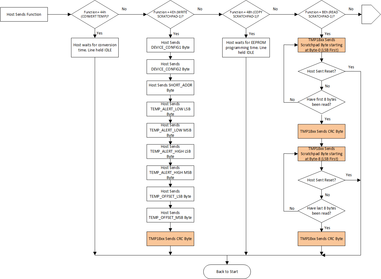
9.4.3.3 Function Phase
Figure 9-22, Figure 9-23 and Figure 9-24 show the function phase that follows the address phase. The host may present different functions during this phase, which is followed by either the host sending data to the device, reading device data, or starting a temperature conversion. Some of the functions may be broadcast to all the devices on the bus using SKIPADDR or OVD SKIPADDR. Read functions must always be unicast with a device selected during the address phase using MATCHADDR, FLEXADDR or OVD MATCHADDR. For cases, where there is a single device on the bus, the device address selection may be skipped.
 Figure 9-22 Function Phase Flowchart for
Register Space