SBOS466B December   2009  – December 2018 TMP20

PRODUCTION DATA.  

  1. Features
  2. Applications
  3. Description
    1.     Device Block Diagram
    2.     Device Quiescent Current Over Temperature
  4. Revision History
  5. Pin Configuration and Functions
    1.     Pin Functions
  6. Specifications
    1. 6.1 Absolute Maximum Ratings
    2. 6.2 ESD Ratings
    3. 6.3 Recommended Operating Conditions
    4. 6.4 Thermal Information
    5. 6.5 Electrical Characteristics
    6. 6.6 Typical Characteristics
  7. Detailed Description
    1. 7.1 Overview
    2. 7.2 Functional Block Diagram
    3. 7.3 Feature Description
      1. 7.3.1 Transfer Function
        1. 7.3.1.1 Example 1
    4. 7.4 Device Functional Modes
  8. Application and Implementation
    1. 8.1 Application Information
      1. 8.1.1 Output Drive and Capacitive Loads
    2. 8.2 Typical Application
      1. 8.2.1 Design Requirements
      2. 8.2.2 Detailed Design Procedure
      3. 8.2.3 Application Curves
  9. Power Supply Recommendations
  10. 10Layout
    1. 10.1 Layout Guidelines
    2. 10.2 Layout Example
  11. 11Device and Documentation Support
    1. 11.1 Device Support
      1. 11.1.1 TINA-TI (Free Download Software)
        1. 11.1.1.1 Using TINA-TI SPICE-Based Analog Simulation Program with the TMP20
      2. 11.1.2 Development Support
    2. 11.2 Receiving Notification of Documentation Updates
    3. 11.3 Community Resources
    4. 11.4 Trademarks
    5. 11.5 Electrostatic Discharge Caution
    6. 11.6 Glossary
  12. 12Mechanical, Packaging, and Orderable Information

Package Options

Mechanical Data (Package|Pins)
Thermal pad, mechanical data (Package|Pins)
Orderable Information

Pin Configuration and Functions

DRL Package
6-Pin SOT-563
Top View
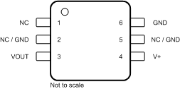
TMP20 TMP20_DRL_pinout.gif
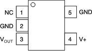
DCK Package
5-Pin SC70
Top View
TMP20 po_dck_bos466.gif
NC- no internal connection

Pin Functions

PIN I/O DESCRIPTION
NAME DRL (SOT-563) DCK (SC70)
GND 6 5 Ground pin
NC 1 1 This pin must be grounded or left floating. See Layout Example for more information.
NC / GND 2, 5 2 This pin must be grounded or left floating. For best thermal response, connect to GND plane. See Layout Example for more information.
VOUT 3 3 O Analog output
V+ 4 4 I Positive supply voltage