SCDS390A September   2018  – December 2018 TMUX1511

PRODUCTION DATA.  

  1. Features
  2. Applications
  3. Description
    1.     Device Images
      1.      Application Example
      2.      Block Diagram
  4. Revision History
  5. Pin Configuration and Functions
    1.     Pin Functions
  6. Specifications
    1. 6.1 Absolute Maximum Ratings
    2. 6.2 ESD Ratings
    3. 6.3 Recommended Operating Conditions
    4. 6.4 Thermal Information
    5. 6.5 Electrical Characteristics
    6. 6.6 Dynamic Characteristics
    7. 6.7 Timing Requirements
    8. 6.8 Typical Characteristics
      1. 6.8.1 Eye Diagrams
  7. Parameter Measurement Information
    1. 7.1  On-Resistance
    2. 7.2  Off-Leakage Current
    3. 7.3  On-Leakage Current
    4. 7.4  IPOFF Leakage Current
    5. 7.5  Transition Time
    6. 7.6  TON (VDD) and TOFF (VDD) Time
    7. 7.7  Propagation Delay
    8. 7.8  Skew
    9. 7.9  Charge Injection
    10. 7.10 Capacitance
    11. 7.11 Off Isolation
    12. 7.12 Channel-to-Channel Crosstalk
    13. 7.13 Bandwidth
  8. Detailed Description
    1. 8.1 Overview
    2. 8.2 Functional Block Diagram
    3. 8.3 Feature Description
      1. 8.3.1 Bidirectional Operation
      2. 8.3.2 Beyond Supply Operation
      3. 8.3.3 1.8 V Logic Compatible Inputs
      4. 8.3.4 Powered-off Protection
      5. 8.3.5 Fail-Safe Logic
      6. 8.3.6 Low Capacitance
      7. 8.3.7 Integrated Pull-Down Resistors
    4. 8.4 Device Functional Modes
    5. 8.5 Truth Tables
  9. Application and Implementation
    1. 9.1 Application Information
    2. 9.2 Typical Application
      1. 9.2.1 Protocol / Signal Isolation
        1. 9.2.1.1 Design Requirements
        2. 9.2.1.2 Detailed Design Procedure
        3. 9.2.1.3 Application Curves
      2. 9.2.2 Transimpedance Amplifier Feedback Control
        1. 9.2.2.1 Design Requirements
        2. 9.2.2.2 Detailed Design Procedure
        3. 9.2.2.3 Application Curves
  10. 10Power Supply Recommendations
  11. 11Layout
    1. 11.1 Layout Guidelines
    2. 11.2 Layout Example
  12. 12Device and Documentation Support
    1. 12.1 Documentation Support
      1. 12.1.1 Related Documentation
    2. 12.2 Receiving Notification of Documentation Updates
    3. 12.3 Community Resources
    4. 12.4 Trademarks
    5. 12.5 Electrostatic Discharge Caution
    6. 12.6 Glossary
  13. 13Mechanical, Packaging, and Orderable Information

Package Options

Mechanical Data (Package|Pins)
Thermal pad, mechanical data (Package|Pins)
Orderable Information

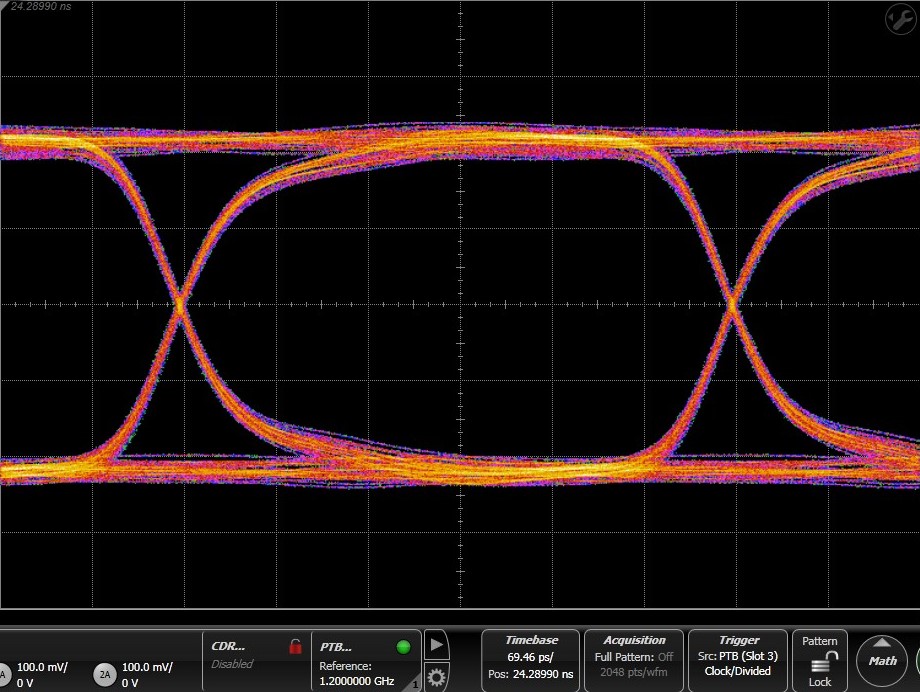
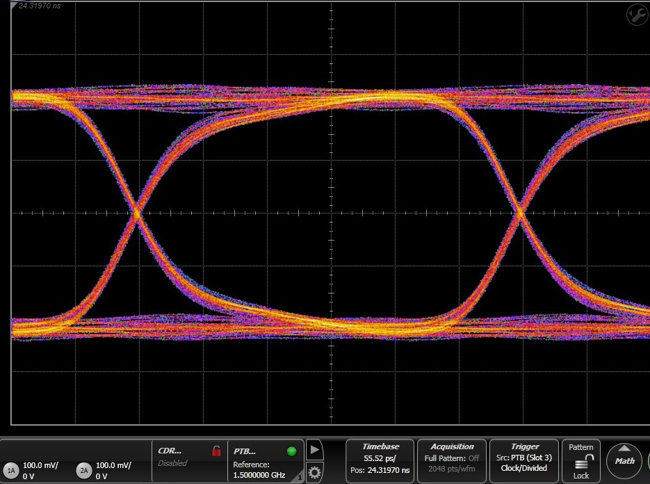
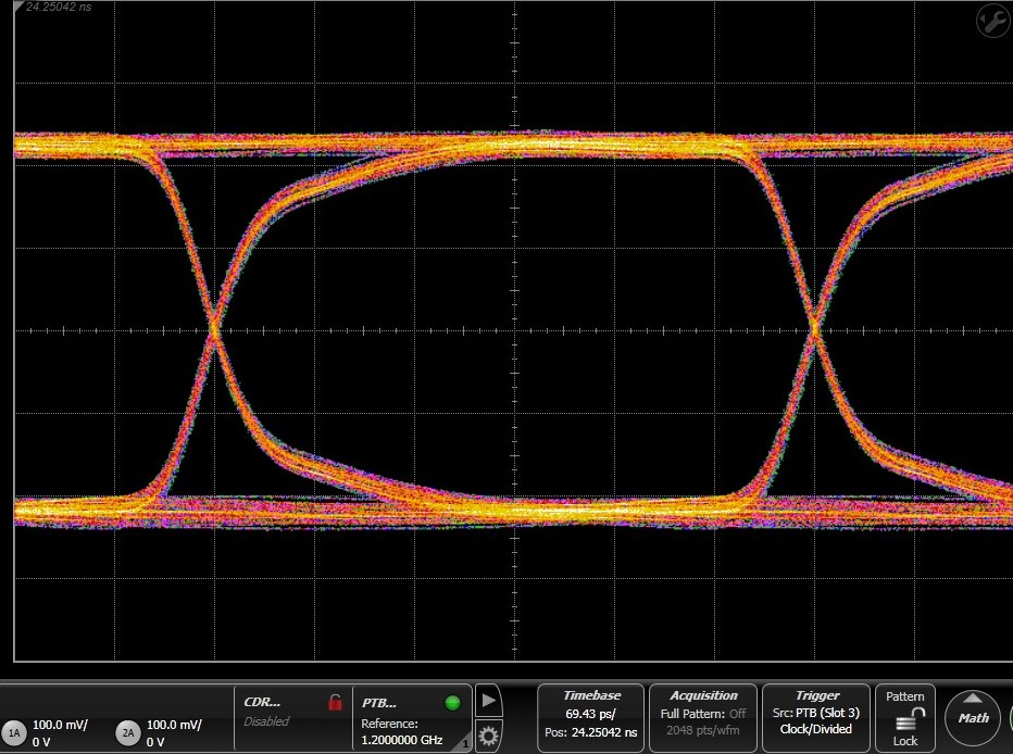
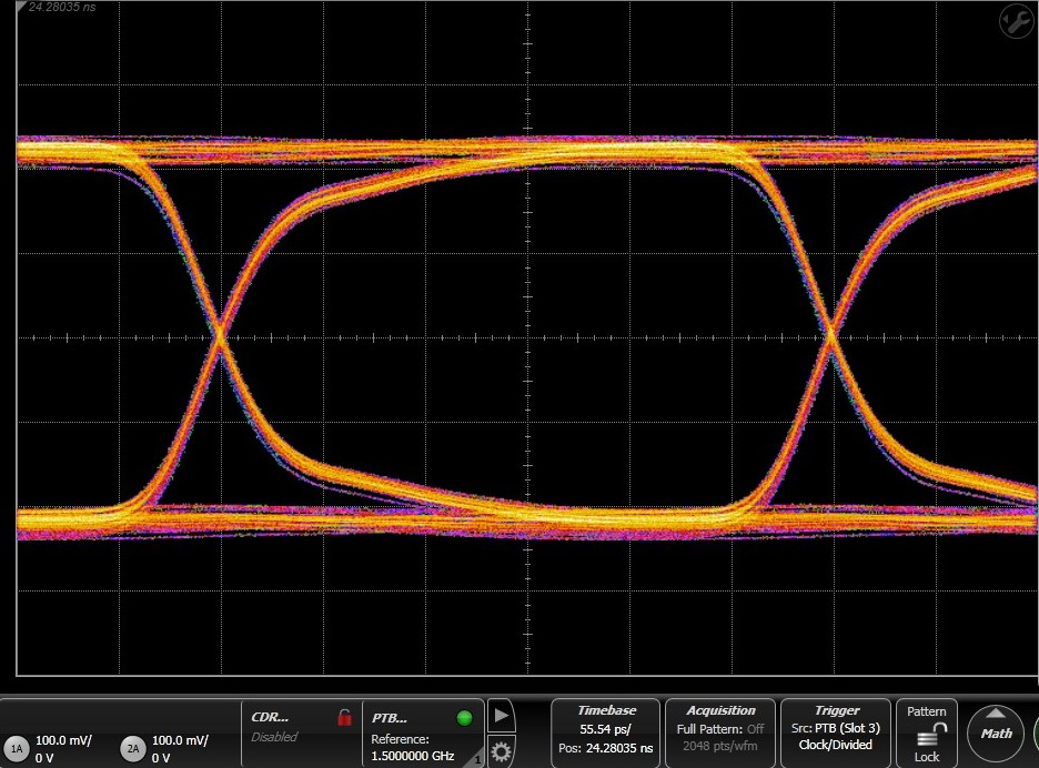
Eye Diagrams

TMUX1511 TMUX1511RSV_eye_D1D2_2p4Gbps.jpg
TA = 25°C
Bias = 1.5 V
50 Ω Termination
Figure 23. Eye Pattern: 2.4 Gbps
TMUX1511 TMUX1511RSV_eye_D1D2_3Gbps.jpg
TA = 25°C
Bias = 1.5 V
50 Ω Termination
Figure 25. Eye Pattern: 3 Gbps
TMUX1511 TMUX1511RSV_eye_thru_2p4Gbps.jpg
TA = 25°C
Bias = 1.5 V
50 Ω Termination
Figure 24. Eye Pattern: 2.4 Gbps Through Path
TMUX1511 TMUX1511RSV_eye_thru_3Gbps.jpg
TA = 25°C
Bias = 1.5 V
50 Ω Termination
Figure 26. Eye Pattern: 3 Gbps Through Path