SCDS457B May 2023 – July 2024 TMUX4827
PRODUCTION DATA
- 1
- 1 Features
- 2 Applications
- 3 Description
- 4 Pin Configuration and Functions
- 5 Specifications
-
6 Parameter Measurement Information
- 6.1 On-Resistance
- 6.2 On-Leakage Current
- 6.3 Off-Leakage Current
- 6.4 Power-Off Leakage Current
- 6.5 Propagation Delay
- 6.6 tON (VDD) and tOFF (VDD) Time
- 6.7 Transition Time
- 6.8 Break-Before-Make
- 6.9 THD + Noise
- 6.10 Power Supply Rejection Ratio (PSRR)
- 6.11 Charge Injection
- 6.12 Bandwidth
- 6.13 Off Isolation
- 6.14 Crosstalk
- 7 Detailed Description
- 8 Application and Implementation
- 9 Device and Documentation Support
- 10Revision History
- 11Mechanical, Packaging, and Orderable Information
Package Options
Refer to the PDF data sheet for device specific package drawings
Mechanical Data (Package|Pins)
- YBH|9
Thermal pad, mechanical data (Package|Pins)
Orderable Information
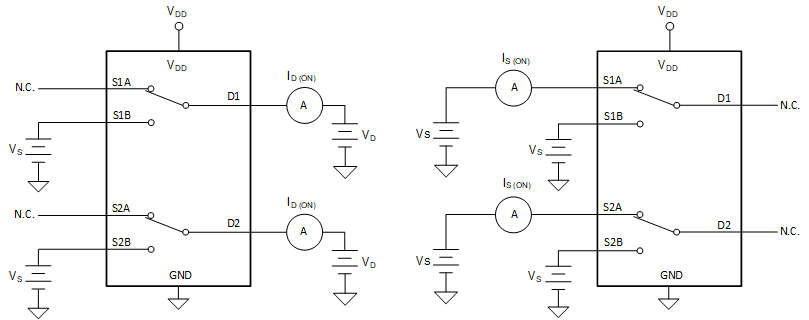
6.2 On-Leakage Current
Source on-leakage current is defined as the leakage current flowing into or out of the source pin when the switch is on. This current is denoted by the symbol IS(ON). Drain on-leakage current is defined as the leakage current flowing into or out of the drain pin when the switch is on. This current is denoted by the symbol ID(ON). Either the source pin or drain pin is left floating during the measurement. Figure 6-2 shows the circuit used for measuring the on-leakage current, denoted by IS(ON) or ID(ON).
 Figure 6-2 On-Leakage
Measurement Setup